Search
Search Lectures
search
864 videos

SSCD IIT Kanpur
Lecture 1: Use of Taylor series to deal with devices having non-linear I-V characteristics
EE 210: Microelectronics I, 2022

SSCD IIT Kanpur
Lecture 2: Relating incremental model of a diode with its operating point.
EE 210: Microelectronics I, 2022

SSCD IIT Kanpur
Lecture 3: Relating the small signal equivalent to the tangent of the I-V characteristics
EE 210: Microelectronics I, 2022

SSCD IIT Kanpur
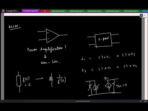
Lecture 4: Can an LTI network generate power gain?
EE 210: Microelectronics I, 2022

SSCD IIT Kanpur
Lecture 5: Requirement of non-linearity for power amplification
EE 210: Microelectronics I, 2022

SSCD IIT Kanpur
Lecture 6: Network theory; revisiting KCL, KVL, substitution theorem
EE 210: Microelectronics I, 2022

SSCD IIT Kanpur
Lecture 7: Network theory; Thevenin's theorem, source substitution, Tellegen's theorem
EE 210: Microelectronics I, 2022

SSCD IIT Kanpur
Lecture 8: Proof of reciprocity theorem; introduction to two-port network
EE 210: Microelectronics I, 2022

SSCD IIT Kanpur
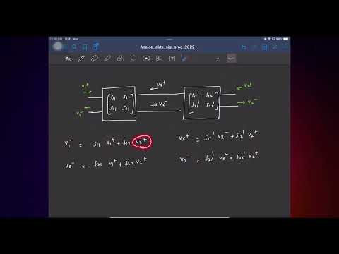
Lecture 9: Necessary y-parameter conditions for amplification
EE 210: Microelectronics I, 2022

SSCD IIT Kanpur
Lecture 10: An elementary introduction to physics of semiconductor devices; PN junction diode
EE 210: Microelectronics I, 2022

SSCD IIT Kanpur
Lecture 11: Introduction to MOS structure
EE 210: Microelectronics I, 2022

SSCD IIT Kanpur
Lecture 12: Introduction to MOSFET structure
EE 210: Microelectronics I, 2022

SSCD IIT Kanpur
Lecture 13: Introduction to I-V characteristics of in a MOSFET, and its relation with y-parameters
EE 210: Microelectronics I, 2022

SSCD IIT Kanpur
Lecture 14: Use of MOSFET in saturation region for amplification
EE 210: Microelectronics I, 2022

SSCD IIT Kanpur
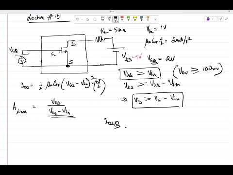
Lecture 15: Synthesis of an amplifier while taking biasing into account
EE 210: Microelectronics I, 2022

SSCD IIT Kanpur
Lecture 16: Swing limits in a common source amplifier
EE 210: Microelectronics I, 2022
SSCD IIT Kanpur
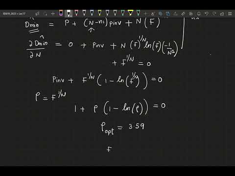
Lecture 17: Biasing a common source amplifier for maximum input swing
EE 210: Microelectronics I, 2022
SSCD IIT Kanpur
Lecture 18: Replacing a battery with a capacitor to bias a common source amplifier
EE 210: Microelectronics I, 2022

SSCD IIT Kanpur
Lecture 19: Finding the component values to bias a the input of a common source amplifier
EE 210: Microelectronics I, 2022
SSCD IIT Kanpur
Lecture 20: Using coupling capacitor to drive a load without affecting bias points
EE 210: Microelectronics I, 2022

SSCD IIT Kanpur
Lecture 21: Bode plot for common source amplifier; Introduction to constant current biasing.
EE 210: Microelectronics I, 2022

SSCD IIT Kanpur
Lecture 22: Constant current biasing; diode connected transistor
EE 210: Microelectronics I, 2022

SSCD IIT Kanpur
Lecture 23: Constant current bias, by applying current at the source; evolution of a voltage buffer
EE 210: Microelectronics I, 2022

SSCD IIT Kanpur
Lecture 24: Source follower architecture
EE 210: Microelectronics I, 2022

SSCD IIT Kanpur
Lecture 25: Introduction to current mirrors to bias a transistor with constant current
EE 210: Microelectronics I, 2022

SSCD IIT Kanpur
Lecture 26: Biasing a transistor by pushing current into the drain tweaking the source
EE 210: Microelectronics I, 2022

SSCD IIT Kanpur
Lecture 27: Biasing a transistor with current sources contd..
EE 210: Microelectronics I, 2022

SSCD IIT Kanpur
Lecture 28: Synthesis of current controlled current source- Common Gate configuration
EE 210: Microelectronics I, 2022

SSCD IIT Kanpur
Lecture 29: Channel length modulation in MOSFET
EE 210: Microelectronics I, 2022

SSCD IIT Kanpur
Lecture 30: Use of a current buffer to improve voltage gain; Introduction to body effect
EE 210: Microelectronics I, 2022

SSCD IIT Kanpur
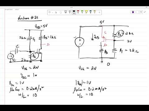
Lecture 31: Effect of channel length modulation on current mirrors
EE 210: Microelectronics I, 2022

SSCD IIT Kanpur
Lecture 32: Synthesis of a stable gain network using negative feedback
EE 210: Microelectronics I, 2022

SSCD IIT Kanpur
Lecture 33: Synthesis of a differential amplifier to realize an error amplifier in a feedback loop.
EE 210: Microelectronics I, 2022

SSCD IIT Kanpur
Lecture 34: Relating a differential amplifier in feedback to a classical negative feedback topology
EE 210: Microelectronics I, 2022

SSCD IIT Kanpur
Lecture 35: Introducing a PMOSFET to realize a gain stage
EE 210: Microelectronics I, 2022

SSCD IIT Kanpur
Lecture 36: Common source amplifier with active load
EE 210: Microelectronics I, 2022

SSCD IIT Kanpur
Lecture 37: Differential amplifier with current mirror load
EE 210: Microelectronics I, 2022

SSCD IIT Kanpur
Lecture 38: Introducing two stage amplifiers and parasitic capacitances
EE 210: Microelectronics I, 2022

SSCD IIT Kanpur
Lecture 39a: Differential amplifier contd..
EE 210: Microelectronics I, 2022

SSCD IIT Kanpur
Lecture 39b: Role of parasitic impedances in stability of a two stage differential amplifier
EE 210: Microelectronics I, 2022

SSCD IIT Kanpur
Lecture 40: Compensating a two stage amplifier by making one pole dominant.
EE 210: Microelectronics I, 2022
SSCD IIT Kanpur
Lecture 41: Frequency compensation of two stage opamp
EE 210: Microelectronics I, 2022

SSCD IIT Kanpur
Lecture 42: Miller Compensated opamp contd..
EE 210: Microelectronics I, 2022

SSCD IIT Kanpur
Lecture 43: Critical differences of BJTs with MOSFETs and analog circuit design using BJTs
EE 210: Microelectronics I, 2022

SSCD IIT Kanpur
Lecture1: Voltage divider - loading effect
EE 610: Analog VLSI design

SSCD IIT Kanpur
Lecture2 - Linearizing a non-linear element
EE 610: Analog VLSI design

SSCD IIT Kanpur
Lecture 4: MOSFET regions, and small signal parameters.
EE 610: Analog VLSI design
SSCD IIT Kanpur
Lecture5: Synthesis of controlled sources using negative feedback
EE 610: Analog VLSI design

SSCD IIT Kanpur
Lecture6: Introduction to negative feedback, with integrator in the loop.
EE 610: Analog VLSI design

SSCD IIT Kanpur
Lecture7: Impact of error injection in a negative feedback loop with an integrator.
EE 610: Analog VLSI design
SSCD IIT Kanpur
Lecture 8: Steady state errors and sinusoidal excitation in negative feedback
EE 610: Analog VLSI design

SSCD IIT Kanpur
Lecture9: Evaluation of Closed loop response from L(s)
EE 610: Analog VLSI design

SSCD IIT Kanpur
Lecture10: Effect of loading while breaking a loop.
EE 610: Analog VLSI design

SSCD IIT Kanpur
Lecture11: Swing limitations and maximum gain in a common source amplifier; Intro to cascode stage
EE 610: Analog VLSI design

SSCD IIT Kanpur
Lecture12: Swing limits continued.
EE 610: Analog VLSI design

SSCD IIT Kanpur
Lecture12 Errata: Correction of swing limits in lecture 12
EE 610: Analog VLSI design
SSCD IIT Kanpur
Lecture13: Amplifier design with constant current biasing.
EE 610: Analog VLSI design

SSCD IIT Kanpur
Lecture14: Constant current biasing contd..
EE 610: Analog VLSI design

SSCD IIT Kanpur
Lecture15: Biasing using constant current source into drain and feedback at source
EE 610: Analog VLSI design

SSCD IIT Kanpur
Lecture16: Introduction to differential amplifier
EE 610: Analog VLSI design

SSCD IIT Kanpur
Lecture17: Input common mode range (ICMR) and common mode rejection ratio (CMRR) in diffamp.
EE 610: Analog VLSI design

SSCD IIT Kanpur
Lecture18: Current mirrors
EE 610: Analog VLSI design

SSCD IIT Kanpur
Lecture19: Active loads using PMOS; Inverters as amplifiers
EE 610: Analog VLSI design

SSCD IIT Kanpur
Lecture 20: Diffamp with current mirror load
EE 610: Analog VLSI design

SSCD IIT Kanpur
Lecture 21: PSRR in differential pairs
EE 610: Analog VLSI design

SSCD IIT Kanpur
Lecture 22: PSRR in difamp in negative feedback
EE 610: Analog VLSI design

SSCD IIT Kanpur
Lecture 23: Swing limits in an opamp in negative feedback
EE 610: Analog VLSI design

SSCD IIT Kanpur
Lecture 24: Introduction of stability issues in multi-pole architectures
EE 610: Analog VLSI design

SSCD IIT Kanpur
Lecture 25: Nyquist criterion and relationship with stability in all-pole systems
EE 610: Analog VLSI design

SSCD IIT Kanpur
Lecture 26: Stability analysis in two stage Miller compensated opamp
EE 610: Analog VLSI design

SSCD IIT Kanpur
Lecture 1: Introduction
EE 698G: Circuit design for frequency and phase synthesis (2023)

SSCD IIT Kanpur
Lecture 2: Flash TDC, PVT variation, Introduction to DLL
EE 698G: Circuit design for frequency and phase synthesis (2023)
SSCD IIT Kanpur
Lecture 3: Variable delay lines
EE 698G: Circuit design for frequency and phase synthesis (2023)

SSCD IIT Kanpur
Lecture 4: Variable delay lines, Phase detectors - Multiplier, S&H, XOR
EE 698G: Circuit design for frequency and phase synthesis (2023)

SSCD IIT Kanpur
Lecture 5: SR latch based PD, PFD
EE 698G: Circuit design for frequency and phase synthesis (2023)

SSCD IIT Kanpur
Lecture 6: Locking in a DLL
EE 698G: Circuit design for frequency and phase synthesis (2023)

SSCD IIT Kanpur
Lecture 7: Locking nonidealities: False locking, harmonic locking, SPO
EE 698G: Circuit design for frequency and phase synthesis (2023)

SSCD IIT Kanpur
Lecture 8: Charge pump implementation
EE 698G: Circuit design for frequency and phase synthesis (2023)

SSCD IIT Kanpur
Lecture 9: Gate-switched charge pump, mismatches, modelling the DLL
EE 698G: Circuit design for frequency and phase synthesis (2023)
SSCD IIT Kanpur
Lecture 10: Small signal phase domain model of the DLL
EE 698G: Circuit design for frequency and phase synthesis (2023)

SSCD IIT Kanpur
Lecture 11: Small signal analysis of DLL (Open and closed loop transfer functions)
EE 698G: Circuit design for frequency and phase synthesis (2023)

SSCD IIT Kanpur
Lecture 12: Discrete time model for the DLL
EE 698G: Circuit design for frequency and phase synthesis (2023)

SSCD IIT Kanpur
Lecture 13: Type-II DLL, DLL applications, noise review
EE 698G: Circuit design for frequency and phase synthesis (2023)

SSCD IIT Kanpur
Lecture 14: Noise review, introduction to phase noise and jitter, jitter definitions
EE 698G: Circuit design for frequency and phase synthesis (2023)

SSCD IIT Kanpur
Lecture 15: Characterizing jitter, relationship between jitter and phase noise, jitter PSD
EE 698G: Circuit design for frequency and phase synthesis (2023)

SSCD IIT Kanpur
Lecture 16: Relationship between phase noise PSD and clock signal PSD; reporting phase noise
EE 698G: Circuit design for frequency and phase synthesis (2023)

SSCD IIT Kanpur
Lecture 17: Phase noise, jitter in inverter, delay line and ring oscillator (qualitative analysis)
EE 698G: Circuit design for frequency and phase synthesis (2023)
SSCD IIT Kanpur
Lecture-18: Introduction to oscillators
EE 698G: Circuit design for frequency and phase synthesis (2023)

SSCD IIT Kanpur
Lecture 1: Introduction and basics of sampling
EE 698I: Mixed-signal IC design (2022)

SSCD IIT Kanpur
Lecture 2: Sampling recap, oversampling, subsampling, and signal reconstruction from its samples
EE 698I: Mixed-signal IC design (2022)

SSCD IIT Kanpur
Lecture 3: Quantization, mid-rise, mid-tread, signal-to-quantization-noise ratio (SQNR)
EE 698I: Mixed-signal IC design (2022)

SSCD IIT Kanpur
Lecture 4: Measuring SQNR (part 1) using the power sp
EE 698I: Mixed-signal IC design (2022)

SSCD IIT Kanpur
Lecture 5: Measuring SQNR (part 2); Basics of discrete Fourier transform (DFT)
EE 698I: Mixed-signal IC design (2022)

SSCD IIT Kanpur
Lecture 6: Measuring SQNR (part 3): Windowing the DFT/FFT; Rectangular & raised-cosine windows
EE 698I: Mixed-signal IC design (2022)

SSCD IIT Kanpur
Lecture 6 (addendum): Time domain explanation for using windowing functions in DFT/FFT
EE 698I: Mixed-signal IC design (2022)

SSCD IIT Kanpur
Lecture 7: ADC performance metrics (part 1); signal to noise ratio variants: SQNR, SNR, SNDR
EE 698I: Mixed-signal IC design (2022)

SSCD IIT Kanpur
Lecture 8: ADC performance metrics (part 2); Integral and differential non-linearity (INL and DNL)
EE 698I: Mixed-signal IC design (2022)

SSCD IIT Kanpur
Lecture 9: Sampling switch implementation; non-idealities: finite ON resistance
EE 698I: Mixed-signal IC design (2022)

SSCD IIT Kanpur
Lecture 10: Gate bootstrapped switch (two variants)
EE 698I: Mixed-signal IC design (2022)

SSCD IIT Kanpur
Lecture 11: Intro to thermal noise; thermal noise during sampling
EE 698I: Mixed-signal IC design (2022)

SSCD IIT Kanpur
Lecture 12: Thermal noise (contd.); Clock jitter and signal dependent sampling
EE 698I: Mixed-signal IC design (2022)

SSCD IIT Kanpur
Lecture 13: Hold-mode feedthrough; Charge injection; Bottom-plate sampling
EE 698I: Mixed-signal IC design (2022)
SSCD IIT Kanpur
Lecture 14: Deriving the switched-capacitor amplifier using Miller effect
EE 698I: Mixed-signal IC design (2022)

SSCD IIT Kanpur
Lecture 15: Settling in switched-capacitor circuits with an OTA
EE 698I: Mixed-signal IC design (2022)

SSCD IIT Kanpur
Lecture 15 (erratum) in swing limits
EE 698I: Mixed-signal IC design (2022)

SSCD IIT Kanpur
Lecture 16: Settling (contd.); Noise in switched-capacitor circuits
EE 698I: Mixed-signal IC design (2022)

SSCD IIT Kanpur
Lecture 17: The switched-capacitor integrator
EE 698I: Mixed-signal IC design (2022)

SSCD IIT Kanpur
Lecture 18: Comparators: Regenerative latch; Strong-arm latch; Offset in latches
EE 698I: Mixed-signal IC design (2022)

SSCD IIT Kanpur
Lecture 19: Latch offset correction: auto-zeroing and calibration
EE 698I: Mixed-signal IC design (2022)

SSCD IIT Kanpur
Lecture 20 (pt. 1): Dynamic preamplifiers; Improving flash ADC resolution: interpolation and folding
EE 698I: Mixed-signal IC design (2022)

SSCD IIT Kanpur
Lecture 20 (pt. 2): Time interleaved ADCs, non-idealities and calibration
EE 698I: Mixed-signal IC design (2022)

SSCD IIT Kanpur
Lecture 22: Pipelined ADC, redundancy to tackle ADC non-idealities
EE 698I: Mixed-signal IC design (2022)

SSCD IIT Kanpur
Lecture 21: Multi-step ADCs
EE 698I: Mixed-signal IC design (2022)
SSCD IIT Kanpur
Lecture 23: Pipelined ADC: redundancy (contd.), and residue amp. non-idealities
EE 698I: Mixed-signal IC design (2022)

SSCD IIT Kanpur
Lecture 24: Deriving the circuit implementation of a pipelined ADC
EE 698I: Mixed-signal IC design (2022)

SSCD IIT Kanpur
Lecture 25: Pipelined ADC: digital calibration of DAC mismatch
EE 698I: Mixed-signal IC design (2022)

SSCD IIT Kanpur
Lecture 1: Course overview, and introduction to bandgap reference
EE 698W: Analog circuits for signal processing (2022)

SSCD IIT Kanpur
Lecture 2: Bandgap reference, introduction to voltage regulators
EE 698W: Analog circuits for signal processing (2022)

SSCD IIT Kanpur
Lecture 3: Low drop-out (LDO) regulators, basics of switching regulator (Buck DC-DC converter)
EE 698W: Analog circuits for signal processing (2022)

SSCD IIT Kanpur
Lecture 5: Variants of the switched RC filter
EE 698W: Analog circuits for signal processing (2022)

SSCD IIT Kanpur
Lecture 6: Bandwidth of the switched RC filter variants; impulse response of linear systems
EE 698W: Analog circuits for signal processing (2022)

SSCD IIT Kanpur
Lecture 7: LPTV systems: Zadeh expansion, harmonic transfer functions of the LPTV bandpass filter
EE 698W: Analog circuits for signal processing (2022)

SSCD IIT Kanpur
Lecture 8: Basics of periodic steady-state (pss), pac and pxf simulation demos in Cadence SpectreRF
EE 698W: Analog circuits for signal processing (2022)

SSCD IIT Kanpur
Lecture 9: Deriving the N-path principle; N-path LPTV systems; Multi-phase Buck converter
EE 698W: Analog circuits for signal processing (2022)

SSCD IIT Kanpur
Lecture 10: N-path/Segmented chopping; Time-interleaved sampling
EE 698W: Analog circuits for signal processing (2022)

SSCD IIT Kanpur
Lecture 11: N-path bandpass filter; deriving the N-path filter, HTFs for the 4-path filter
EE 698W: Analog circuits for signal processing (2022)

SSCD IIT Kanpur
Lecture 12: Differential N-path filter; B.W. calculation; Passive Mixers; N-path filter+Mixer combo
EE 698W: Analog circuits for signal processing (2022)

SSCD IIT Kanpur
Lecture 13: Impedance/admittance conversion matrix of LPTV systems
EE 698W: Analog circuits for signal processing (2022)

SSCD IIT Kanpur
Lecture 14: Harmonic transfer matrix; Conversion matrix-based analysis of LPTV ckts; Intro to noise
EE 698W: Analog circuits for signal processing (2022)

SSCD IIT Kanpur
Lecture 15: Assignment soln; Tellegen's theorem, its extensions; Reciprocity theorem with resistors.
EE 698W: Analog circuits for signal processing (2022)

SSCD IIT Kanpur
Lecture 16: Reciprocity and inter-reciprocity in linear time-invariant (LTI) networks
EE 698W: Analog circuits for signal processing (2022)

SSCD IIT Kanpur
Lecture 17: Nyquist noise theorem and Bode's noise theorem in linear time invariant networks
EE 698W: Analog circuits for signal processing (2022)

SSCD IIT Kanpur
Lecture 18: Using conversion matrices to prove inter-reciprocity in LPTV networks
EE 698W: Analog circuits for signal processing (2022)

SSCD IIT Kanpur
Lecture 19: Inter-reciprocity relation in time domain based on impulse response & signal flow graphs
EE 698W: Analog circuits for signal processing (2022)

SSCD IIT Kanpur
Lecture 20: Inter-reciprocity eg. Chopping; LPTV network with sampled output; Noise in LPTV circuits
EE 698W: Analog circuits for signal processing (2022)

SSCD IIT Kanpur
Lecture 21: Mean-squared noise in LPTV networks with RLC and switches; Intro to transmission lines
EE 698W: Analog circuits for signal processing (2022)

SSCD IIT Kanpur
Lecture 22: Laplace transform based analysis of transmission line; input impedance; reflection coeff
EE 698W: Analog circuits for signal processing (2022)

SSCD IIT Kanpur
Lecture 23: Maximum power transfer; Need for S-parameters; Example problems
EE 698W: Analog circuits for signal processing (2022)
SSCD IIT Kanpur
Lecture 24: S-parameters; Vector network analyzer; Stability in negative feedback systems with zeros
EE 698W: Analog circuits for signal processing (2022)

SSCD IIT Kanpur
Lecture 4: Chopping
EE 698W: Analog circuits for signal processing (2022)

SSCD IIT Kanpur
Lecture 1: Consequences of driving a low-impedance load
EE210-2025 (Analog Electronics)

SSCD IIT Kanpur
Lecture 2: Why do we need a voltage controlled voltage source?
EE210-2025 (Analog Electronics)

SSCD IIT Kanpur
Lecture 3: Need for non-linearity to get power amplification
EE210-2025 (Analog Electronics)

SSCD IIT Kanpur
Lecture 4: Linearizing a non-linear circuit
EE210-2025 (Analog Electronics)

SSCD IIT Kanpur
Lecture 5: Linearizing non-linear elements in a network
EE210-2025 (Analog Electronics)

SSCD IIT Kanpur
Lecture 6: Combining incremental response with the quiescent response
EE210-2025 (Analog Electronics)

SSCD IIT Kanpur
Lecture 7: Finding incremental resistance and introduction to two-ports (incomplete recording)
EE210-2025 (Analog Electronics)

SSCD IIT Kanpur
Lecture 8: Incremental two-port Y-parameters and their usage in understanding controlled sources
EE210-2025 (Analog Electronics)

SSCD IIT Kanpur
Lecture 9: Desirable I-V char of a 2-port-network for amplification (Frozen video after 15:00)
EE210-2025 (Analog Electronics)

SSCD IIT Kanpur
Lecture 10: Visualising mechanical ways of creating an amplifier
EE210-2025 (Analog Electronics)

SSCD IIT Kanpur
Lecture 11: Introduction of MOS structure to control current through a third-terminal
EE210-2025 (Analog Electronics)

SSCD IIT Kanpur
Lecture 12: Intro to I-V char of a MOSFET
EE210-2025 (Analog Electronics)

SSCD IIT Kanpur
Lecture 13: Relating I-V char of a MOSFET (in linear region) to the y-parameters of a two port
EE210-2025 (Analog Electronics)

SSCD IIT Kanpur
Lecture 14: Relating I-V char of a MOSFET (in saturation) to two-port y-parameter model.
EE210-2025 (Analog Electronics)
SSCD IIT Kanpur
Lecture 15: Intro to common-source amplifier
EE210-2025 (Analog Electronics)

SSCD IIT Kanpur
Lecture 16: Estimating swing limits of a sinusoidal input signal when applied to a CS stage
EE210-2025 (Analog Electronics)

SSCD IIT Kanpur
Lecture 17: Max achievable gain in a resistively loaded CS amplifier
EE210-2025 (Analog Electronics)

SSCD IIT Kanpur
Lecture 18: Using a capacitor to help replace multiple voltage sources for biasing
EE210-2025 (Analog Electronics)

SSCD IIT Kanpur
Lecture 19: Relating time-constant to 3dB frequencies in Bode plots
EE210-2025 (Analog Electronics)

SSCD IIT Kanpur
Lecture 20: Biasing a transistor with constant current source
EE210-2025 (Analog Electronics)

SSCD IIT Kanpur
Lecture 21: Biasing a transistor using a current source contd..
EE210-2025 (Analog Electronics)

SSCD IIT Kanpur
Lecture 22: Constant current bias by applying current source/sink to the source of the transistor
EE210-2025 (Analog Electronics)

SSCD IIT Kanpur
Lecture 23: CS amplifier with current source at the source; Introducing the source follower.
EE210-2025 (Analog Electronics)

SSCD IIT Kanpur
Lecture 24: Biasing a transistor with a current source at drain and feedback at source
EE210-2025 (Analog Electronics)

SSCD IIT Kanpur
Lecture 25: Discussion constant current source biasing contd..
EE210-2025 (Analog Electronics)

SSCD IIT Kanpur
Lecture 26: Introduction to channel length modulation and its implications
EE210-2025 (Analog Electronics)

SSCD IIT Kanpur
Lecture 27: Introduction to cascode configuration
EE210-2025 (Analog Electronics)

SSCD IIT Kanpur
Lecture 28: Discussion on cascode (common gate) configuration
EE210-2025 (Analog Electronics)

SSCD IIT Kanpur
Lecture 29: Using PMOS transistor to increase gain of the NMOS common source amplifier
EE210-2025 (Analog Electronics)

SSCD IIT Kanpur
Lecture 30: Introducing PMOS transistor to increase the incremental output resistance in a CS amp.
EE210-2025 (Analog Electronics)
SSCD IIT Kanpur
Lecture 31: Converting an NMOS based network to a PMOS based network
EE210-2025 (Analog Electronics)

SSCD IIT Kanpur
Lecture 32: Using negative feedback to obtain precise gain.
EE210-2025 (Analog Electronics)

SSCD IIT Kanpur
Lecture 33: Using source following to prevent loading while designing negative feedback loop
EE210-2025 (Analog Electronics)

SSCD IIT Kanpur
Lecture 34: Norton equivalent of difference amplifier
EE210-2025 (Analog Electronics)

SSCD IIT Kanpur
Lecture 35: Norton equivalent of a differential amp contd..
EE210-2025 (Analog Electronics)

SSCD IIT Kanpur
Lecture 36: Differential amplifier with a current mirror load
EE210-2025 (Analog Electronics)
SSCD IIT Kanpur
Lecture 37: Analysis of diffamp by splitting inputs into differential and common mode
EE210-2025 (Analog Electronics)

SSCD IIT Kanpur
Lecture 38: Capacitances in a MOSFET and its effects on feedback loop
EE210-2025 (Analog Electronics)

SSCD IIT Kanpur
Lecture 39: Poles in diff-pair and relating UGB of loop gain to -3dB bandwidth of the closed loop
EE210-2025 (Analog Electronics)

SSCD IIT Kanpur
Untitled video
EE210-2025 (Analog Electronics)

SSCD IIT Kanpur
Lecture 41: Introduction to BJT as an amplifying device
EE210-2025 (Analog Electronics)

SSCD IIT Kanpur
Lecture 42: Critical differences of BJT with MOSFET and design steps to handle them
EE210-2025 (Analog Electronics)

SSCD IIT Kanpur
Lecture 1: Substitution theorem revisited
EE210: Analog Electronics - 2023-24

SSCD IIT Kanpur
Lecture 2: Derivation of Thevenin's theorem
EE210: Analog Electronics - 2023-24

SSCD IIT Kanpur
Lecture 3a: How can we ascertain if a source inside a black box is voltage or a current source?
EE210: Analog Electronics - 2023-24

SSCD IIT Kanpur
Lecture 3(b): Ascertaining the type of source inside a box
EE210: Analog Electronics - 2023-24

SSCD IIT Kanpur
Lecture 4: Linearizing a non-linear element
EE210: Analog Electronics - 2023-24

SSCD IIT Kanpur
Lecture 5: Incremental analysis with generic non-linearity
EE210: Analog Electronics - 2023-24

SSCD IIT Kanpur
Lecture 6: Developing a generic framework for small signal equivalent
EE210: Analog Electronics - 2023-24
SSCD IIT Kanpur
Lecture 7: Requirement of non-linearity for power amplification
EE210: Analog Electronics - 2023-24

SSCD IIT Kanpur
Lecture 8: Introduction to non-linear two port network
EE210: Analog Electronics - 2023-24

SSCD IIT Kanpur
Lecture 9: Desirable characteristics of two-port incremental network for amplification
EE210: Analog Electronics - 2023-24

SSCD IIT Kanpur
Lecture 10: Desirable I-V characteristics of a non-linear two port for amplification
EE210: Analog Electronics - 2023-24
SSCD IIT Kanpur
Lecture 11: Relating a mechanical amplifier to an electronic counterpart
EE210: Analog Electronics - 2023-24

SSCD IIT Kanpur
Lecture 12: Evolution of a device needed for amplification
EE210: Analog Electronics - 2023-24

SSCD IIT Kanpur
Lecture 13: Introduction to the I-V char of a p-MOSFET
EE210: Analog Electronics - 2023-24

SSCD IIT Kanpur
Lecture 14: Introduction to the small-signal model of a p-MOSFET
EE210: Analog Electronics - 2023-24
SSCD IIT Kanpur
Lecture 15: Various regions of operation of a P-MOSFET
EE210: Analog Electronics - 2023-24

SSCD IIT Kanpur
Lecture 16a: Biasing a P-MOSFET in saturation region and application of incremental input
EE210: Analog Electronics - 2023-24

SSCD IIT Kanpur
Lecture 16b: Biasing a P-MOSFET in saturation contd...
EE210: Analog Electronics - 2023-24

SSCD IIT Kanpur
Lecture 17: A basic amplifier topology using a PMOS transistor
EE210: Analog Electronics - 2023-24

SSCD IIT Kanpur
Lecture 18: Use to a capacitor to replace a floating battery for biasing
EE210: Analog Electronics - 2023-24

SSCD IIT Kanpur
Lecture 19: Finding the values of the capacitances to be used in a common source amplifier
EE210: Analog Electronics - 2023-24

SSCD IIT Kanpur
Lecture 20: Introduction of an NMOS transistor and its similarities with the PMOS device
EE210: Analog Electronics - 2023-24

SSCD IIT Kanpur
Lecture 21: Introduction to constant current biasing
EE210: Analog Electronics - 2023-24

SSCD IIT Kanpur
Lecture 22: Constant current source biasing
EE210: Analog Electronics - 2023-24

SSCD IIT Kanpur
Lecture 23: Constant current bias, by applying current at the source.
EE210: Analog Electronics - 2023-24

SSCD IIT Kanpur
Lecture 24: Using a constant current source to bias a transistor
EE210: Analog Electronics - 2023-24

SSCD IIT Kanpur
Lecture 25: Design of controlled sources using MOSFETs
EE210: Analog Electronics - 2023-24

SSCD IIT Kanpur
Lecture 26: Synthesis of a common-drain and a common-gate configuration
EE210: Analog Electronics - 2023-24

SSCD IIT Kanpur
Lecture 27: Channel length modulation in MOSFET
EE210: Analog Electronics - 2023-24

SSCD IIT Kanpur
Lecture 28: Use of a current buffer to improve voltage gain; Introduction to body effect
EE210: Analog Electronics - 2023-24

SSCD IIT Kanpur
Lecture 29: Use of a current buffer (Common gate config) contd..
EE210: Analog Electronics - 2023-24

SSCD IIT Kanpur
Lecture 30: Introduction to current mirrors and the effect of channel length modulation
EE210: Analog Electronics - 2023-24

SSCD IIT Kanpur
Lecture 31: Cascode current mirrors
EE210: Analog Electronics - 2023-24

SSCD IIT Kanpur
Lecture 32: Wide-swing current mirror
EE210: Analog Electronics - 2023-24

SSCD IIT Kanpur
Lecture 33: Designing an amplifier using negative feedback
EE210: Analog Electronics - 2023-24

SSCD IIT Kanpur
Lecture 34: Introduction to differential amplifier for use in negative feedback loop
EE210: Analog Electronics - 2023-24

SSCD IIT Kanpur
Lecture 35: Loop gain of a negative feedback loop using a differential amplifier
EE210: Analog Electronics - 2023-24

SSCD IIT Kanpur
Lecture 36: Differential amplifier with current mirror load
EE210: Analog Electronics - 2023-24

SSCD IIT Kanpur
Lecture 37: Capacitances in a MOS transistor and its effects on amplifier
EE210: Analog Electronics - 2023-24

SSCD IIT Kanpur
Lecture 38: Relation between open loop gain and the the closed loop response
EE210: Analog Electronics - 2023-24

SSCD IIT Kanpur
Lecture 39: Relating the damping factor of a second order closed loop system to phase margin of L(s)
EE210: Analog Electronics - 2023-24

SSCD IIT Kanpur
Lecture 40: Loop gain of two stage amplifier and its impact on stability
EE210: Analog Electronics - 2023-24

SSCD IIT Kanpur
Lecture 41: Stability of two stage opamps and introduction to Miller compensation
EE210: Analog Electronics - 2023-24

SSCD IIT Kanpur
EE370 Lec1: Overview of digital design implementation (Introductory lecture)
EE370: Digital Electronics (2025)

SSCD IIT Kanpur
EE370 lec2: Verilog (I)
EE370: Digital Electronics (2025)

SSCD IIT Kanpur
EE370 lec3: Verilog - (II)
EE370: Digital Electronics (2025)

SSCD IIT Kanpur
EE370 lec4: Verilog - (III)
EE370: Digital Electronics (2025)

SSCD IIT Kanpur
EE370 lec5: Verilog (IV)
EE370: Digital Electronics (2025)

SSCD IIT Kanpur
EE370 lec6: Mealy vs Moore state machines
EE370: Digital Electronics (2025)

SSCD IIT Kanpur
EE370 lec7: State minimization in FSM, FSMD
EE370: Digital Electronics (2025)

SSCD IIT Kanpur
EE370 lec 8 (1) : Introduction to FSM and datapath
EE370: Digital Electronics (2025)

SSCD IIT Kanpur
EE370 lec 8 (2): FSMD for greatest common divisor computation
EE370: Digital Electronics (2025)

SSCD IIT Kanpur
EE370 lec11(1) : Design of controller for a faster algorithm for GCD computation
EE370: Digital Electronics (2025)

SSCD IIT Kanpur
EE370 lec11(2) : Verilog implementation of GCD algorithm
EE370: Digital Electronics (2025)

SSCD IIT Kanpur
EE370 lec12: Timing analysis in a digital design
EE370: Digital Electronics (2025)

SSCD IIT Kanpur
EE370 lec13: Static timing analysis (II)
EE370: Digital Electronics (2025)

SSCD IIT Kanpur
EE370 lec14 (1): Review of an FSMD for modulo operation
EE370: Digital Electronics (2025)

SSCD IIT Kanpur
EE370 lec14( 2): STA with contamination and propagation delays
EE370: Digital Electronics (2025)

SSCD IIT Kanpur
EE370 lec15: ROM, PAL, PLA
EE370: Digital Electronics (2025)

SSCD IIT Kanpur
EE370 lec16( 1): Tutorial problem of setup, hold and clk-to-q delays of a D-flipflop
EE370: Digital Electronics (2025)

SSCD IIT Kanpur
EE370 lec16( 2): Wired OR in ROM (one implementation), SPLD, CPLD, FPGA
EE370: Digital Electronics (2025)

SSCD IIT Kanpur
EE370 lec17: Transistor as a switch
EE370: Digital Electronics (2025)
SSCD IIT Kanpur
EE370 lec19: Capacitance in a MOSFET
EE370: Digital Electronics (2025)

SSCD IIT Kanpur
EE370 lec21: Voltage Transfer Characteristics of a CMOS inverter
EE370: Digital Electronics (2025)

SSCD IIT Kanpur
EE370 lec22: Mid-point voltage in a CMOS inverter
EE370: Digital Electronics (2025)

SSCD IIT Kanpur
EE370 lec23: Mid-point voltage (II), Noise margin from VTC
EE370: Digital Electronics (2025)

SSCD IIT Kanpur
EE370 lec24: Delays in a CMOS inverter (I)
EE370: Digital Electronics (2025)
SSCD IIT Kanpur
EE370 lec25: Delays in a CMOS inverter (II)
EE370: Digital Electronics (2025)

SSCD IIT Kanpur
EE370 lec26(1): Delays in a CMOS inverter (III)
EE370: Digital Electronics (2025)

SSCD IIT Kanpur
EE370 lec26(2): Elmore Delay
EE370: Digital Electronics (2025)

SSCD IIT Kanpur
EE370 lec27: Power consumption in CMOS inverters
EE370: Digital Electronics (2025)

SSCD IIT Kanpur
EE370 lec28: Trade-offs in optimizing power consumption in a CMOS inverter
EE370: Digital Electronics (2025)
SSCD IIT Kanpur
EE370 lec29: Sizing an inverter chain for optimal delay
EE370: Digital Electronics (2025)
SSCD IIT Kanpur
EE370 lec30: Overview of CMOS inverter layout, combinational logic
EE370: Digital Electronics (2025)

SSCD IIT Kanpur
EE370 lec31: Sizing transistors in combinational circuits
EE370: Digital Electronics (2025)

SSCD IIT Kanpur
EE370 lec32: Propagation and contamination delays in a combinational circuit
EE370: Digital Electronics (2025)

SSCD IIT Kanpur
EE370 lec33(1): Fall propagation delay in N-input NAND gate
EE370: Digital Electronics (2025)

SSCD IIT Kanpur
EE370 lec33(2): Deriving PUN from PDN using graphs
EE370: Digital Electronics (2025)

SSCD IIT Kanpur
EE370 lec33(3): Pass transistor logic
EE370: Digital Electronics (2025)

SSCD IIT Kanpur
EE370 lec34(1): Pass transistor logic-II
EE370: Digital Electronics (2025)

SSCD IIT Kanpur
EE370 lec34(2): Latches and flip-flops
EE370: Digital Electronics (2025)

SSCD IIT Kanpur
EE370 lec35: Latch implementation using transmission gates; Bistable element
EE370: Digital Electronics (2025)

SSCD IIT Kanpur
EE370 lec36(1): Timing parameters of a flipflop built using TGs and bistable elements
EE370: Digital Electronics (2025)

SSCD IIT Kanpur
EE370 lec36(2): Introduction to adder circuits
EE370: Digital Electronics (2025)

SSCD IIT Kanpur
EE370 lec37: Ripple carry adder
EE370: Digital Electronics (2025)

SSCD IIT Kanpur
EE370 lec38: Carry bypass adder
EE370: Digital Electronics (2025)

SSCD IIT Kanpur
EE370 lec39(1): Carry select adder
EE370: Digital Electronics (2025)

SSCD IIT Kanpur
EE370 lec39(2): EE370 done! What next?
EE370: Digital Electronics (2025)

Dr. Shubham Sahay
Lecture - 1 Introduction and Historical Perspective
EE370A: Digital Electronics

Dr. Shubham Sahay
Lecture - 2 State-of-the-art and a peek into the future
EE370A: Digital Electronics

Dr. Shubham Sahay
Lecture - 3 Quality Metrics for design
EE370A: Digital Electronics

Dr. Shubham Sahay
Lecture - 4 Quality Metrics - Performance and Power
EE370A: Digital Electronics

Dr. Shubham Sahay
Lecture - 5 Inverter implementation with switch and resistor
EE370A: Digital Electronics

Dr. Shubham Sahay
Lecture - 6 MOSFETs as Switch
EE370A: Digital Electronics

Dr. Shubham Sahay
Lecture - 7 Inverter with N-MOSFETs: VTC
EE370A: Digital Electronics

Dr. Shubham Sahay
Lecture - 8 Inverters with NMOSFETs: power and delay
EE370A: Digital Electronics

Dr. Shubham Sahay
Lecture - 9 Inverters with MOSFET-based load
EE370A: Digital Electronics

Dr. Shubham Sahay
Lecture - 10 CMOS inverter: static characteristics
EE370A: Digital Electronics

Dr. Shubham Sahay
Lecture-11 CMOS Inverter: Dynamic characteristics
EE370A: Digital Electronics

Dr. Shubham Sahay
Lecture - 12 CMOS inverters: Power dissipation
EE370A: Digital Electronics

Dr. Shubham Sahay
Lecture 13 - Chain of CMOS inverters
EE370A: Digital Electronics

Dr. Shubham Sahay
Lecture - 14 Introduction to combinational circuits
EE370A: Digital Electronics

Dr. Shubham Sahay
Lecture 15 - Sizing Combinational circuits
EE370A: Digital Electronics
Dr. Shubham Sahay
Lecture 16 - Logical effort method
EE370A: Digital Electronics

Dr. Shubham Sahay
Lecture 17 - Switching Activity
EE370A: Digital Electronics

Dr. Shubham Sahay
Lecture - 18 Alternate Logic design techniques
EE370A: Digital Electronics

Dr. Shubham Sahay
Lecture - 19 Mitigating issues with Pass transistor logic
EE370A: Digital Electronics

Dr. Shubham Sahay
Lecture 20 - Dynamic CMOS design
EE370A: Digital Electronics

Dr. Shubham Sahay
Lecture 21 - Sequential circuits: Static Timing Analysis
EE370A: Digital Electronics

Dr. Shubham Sahay
Lecture 22 - Bistable elements and Latches
EE370A: Digital Electronics

Dr. Shubham Sahay
Lecture 23 - Clock skew and SR flipflop
EE370A: Digital Electronics

Dr. Shubham Sahay
Lecture 24 - Dynamic registers and Pipelining
EE370A: Digital Electronics

Dr. Shubham Sahay
Lecture 25 - Multivibrator circuits
EE370A: Digital Electronics

Dr. Shubham Sahay
Lecture 26 - Memory Organization
EE370A: Digital Electronics

Dr. Shubham Sahay
Lecture 27 - Memory Design: Architectural perspective
EE370A: Digital Electronics

Dr. Shubham Sahay
Lecture 28 - Read and Write in SRAM cells
EE370A: Digital Electronics

Dr. Shubham Sahay
Lecture 29 - Read-write conflict in SRAM
EE370A: Digital Electronics

Dr. Shubham Sahay
Lecture 30 - Dynamic RAM
EE370A: Digital Electronics

SSCD IIT Kanpur
Lecture 1: Need for nonlinearity, Analysis of one-port nonlinear device
EE610 (2024): Analog VLSI circuits

SSCD IIT Kanpur
Lecture 2: Small-signal linear analysis for a one-port network, Analysis of a 2-port network
EE610 (2024): Analog VLSI circuits

SSCD IIT Kanpur
Lecture 3: MOSFET I-V characteristics; Identifying region of operation for amplification
EE610 (2024): Analog VLSI circuits

SSCD IIT Kanpur
Lecture 4: Building an amplifier using a MOSFET
EE610 (2024): Analog VLSI circuits

SSCD IIT Kanpur
Lecture 5: Input signal swing limits in a common source amplifier
EE610 (2024): Analog VLSI circuits

SSCD IIT Kanpur
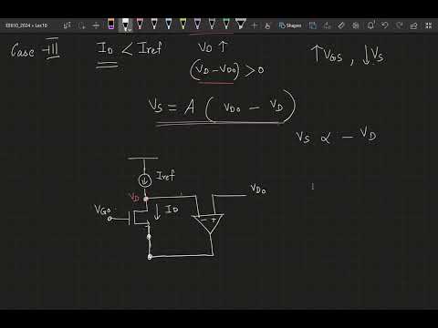
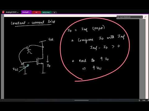
Lecture 6: Constant current bias in common source amplifier
EE610 (2024): Analog VLSI circuits

SSCD IIT Kanpur
Lecture 7: Common source amplifier with constant current bias - II
EE610 (2024): Analog VLSI circuits

SSCD IIT Kanpur
Lecture 8: Common source amplifier with constant current bias-III
EE610 (2024): Analog VLSI circuits

SSCD IIT Kanpur
Lecture 9: Negative feedback loops
EE610 (2024): Analog VLSI circuits
SSCD IIT Kanpur
Lecture 10(1): Common source amplifier with constant current bias - IV
EE610 (2024): Analog VLSI circuits

SSCD IIT Kanpur
Lecture 10(2): Implementing a VCVS using a transistor
EE610 (2024): Analog VLSI circuits

SSCD IIT Kanpur
Lecture 11: Implementing a VCCS using a transistor
EE610 (2024): Analog VLSI circuits

SSCD IIT Kanpur
Lecture 12(1): Implementing a CCCS using a transistor
EE610 (2024): Analog VLSI circuits

SSCD IIT Kanpur
Lecture 12 (2): Implementing a CCVS using a transistor
EE610 (2024): Analog VLSI circuits

SSCD IIT Kanpur
Lecture 12 (3): Summary: VCVS, VCCS, CCCS and CCVS using an NMOS transistor
EE610 (2024): Analog VLSI circuits

SSCD IIT Kanpur
Lecture 13 (1): Impedance looking into the drain of a transistor
EE610 (2024): Analog VLSI circuits

SSCD IIT Kanpur
Lecture 13 (2): Impedance looking at the source of the transistor
EE610 (2024): Analog VLSI circuits

SSCD IIT Kanpur
Lecture 13 (3): Quick and approximate analysis of a circuit with multiple controlled sources.
EE610 (2024): Analog VLSI circuits

SSCD IIT Kanpur
Lecture 14: Building circuits with PMOS transistor
EE610 (2024): Analog VLSI circuits

SSCD IIT Kanpur
Lecture 14 (2): Condition for saturation region in an NMOS transistor vs PMOS transistor
EE610 (2024): Analog VLSI circuits

SSCD IIT Kanpur
Lecture 15: Common source amplifier with an active load
EE610 (2024): Analog VLSI circuits

SSCD IIT Kanpur
Lecture 16: CMOS inverter, differential amplifier-I
EE610 (2024): Analog VLSI circuits

SSCD IIT Kanpur
Lecture 17: Differential amplifier - II
EE610 (2024): Analog VLSI circuits

SSCD IIT Kanpur
Lecture 18: The 5-transistor differential amplifier: Differential & common-mode gain
EE610 (2024): Analog VLSI circuits

SSCD IIT Kanpur
Lecture 19: DC operating point and input common-mode range in a five-transistor OTA
EE610 (2024): Analog VLSI circuits

SSCD IIT Kanpur
Lecture 20: Relevance of input common-mode range & output limits; Two-stage OTA & biasing
EE610 (2024): Analog VLSI circuits

SSCD IIT Kanpur
Lecture 21: Negative feedback and loop gain
EE610 (2024): Analog VLSI circuits

SSCD IIT Kanpur
Lecture 22: Differences between voltage & current feedback; 1st order system in negative feedback
EE610 (2024): Analog VLSI circuits

SSCD IIT Kanpur
Lecture 23: 2nd-order system in negative feedback; Types of damping; Deriving phase margin
EE610 (2024): Analog VLSI circuits

SSCD IIT Kanpur
Lec 1(1): Why non-linear ckts? 1-port amp. I-V char; operating point & small-signal linear eq. ckt
EE610: Analog IC design-1 (2025)

SSCD IIT Kanpur
Lec 1(2): I-V char. of 2-port non-linear network to work as an amp.; Small-signal linear circuit
EE610: Analog IC design-1 (2025)

SSCD IIT Kanpur
Lec 2(1): A 45 minute recap/intro to MOSFET: from the point of view of building analog circuits
EE610: Analog IC design-1 (2025)
SSCD IIT Kanpur
Lec 2(2): Common-source amplifier: Biasing the transistor
EE610: Analog IC design-1 (2025)

SSCD IIT Kanpur
Lec 3(1): Constant-voltage biasing for a common-source amplifier
EE610: Analog IC design-1 (2025)
SSCD IIT Kanpur
Lec 3(2): Motivation for constant-current biasing; Drain and source feedback
EE610: Analog IC design-1 (2025)

SSCD IIT Kanpur
Lec 4(1): Biasing common-source amplifier with source feedback; pMOS common-source amplifier example
EE610: Analog IC design-1 (2025)

SSCD IIT Kanpur
Lec 4(2): Common-drain and common-gate; Resistance looking into the source of a transistor
EE610: Analog IC design-1 (2025)

SSCD IIT Kanpur
Lec 5: Evolution of differential amplifier (from common-source to 5-transistor amplifier)
EE610: Analog IC design-1 (2025)

SSCD IIT Kanpur
Lec 6(1): Cascode current source; Recap of some common impedances
EE610: Analog IC design-1 (2025)

SSCD IIT Kanpur
Lec 6(2): The 5-transistor amplifier: DC operating point
EE610: Analog IC design-1 (2025)

SSCD IIT Kanpur
Lec 6(3): The 5-transitor amplifier: Output resistance & Short-circuit transconductance
EE610: Analog IC design-1 (2025)

SSCD IIT Kanpur
Lec 7(1): 5-transistor differential amplifier: Is it really an opamp?
EE610: Analog IC design-1 (2025)

SSCD IIT Kanpur
Lec 7(2): The 5-T OTA: Common-mode gain & differential mode gain
EE610: Analog IC design-1 (2025)

SSCD IIT Kanpur
Lec 7(3): The 5-T OTA: Resistance looking into different nodes
EE610: Analog IC design-1 (2025)

SSCD IIT Kanpur
Lec 7(4): Relevance on the range for input common-mode and output
EE610: Analog IC design-1 (2025)

SSCD IIT Kanpur
Lec 8(1): Input common-mode range & output swing limits in the 5-T OTA
EE610: Analog IC design-1 (2025)

SSCD IIT Kanpur
Lec 8(2): How to learn & analyze analog circuits? eg of flipped & super source follower
EE610: Analog IC design-1 (2025)

SSCD IIT Kanpur
Lec 9(1): Difference between a VCVS and VCCS in negative feedback
EE610: Analog IC design-1 (2025)

SSCD IIT Kanpur
Lec 9(2): Understanding slewing & slew rate in the 5-T OTA
EE610: Analog IC design-1 (2025)

SSCD IIT Kanpur
Lec 9(3): Introduction to telescopic cascode
EE610: Analog IC design-1 (2025)

SSCD IIT Kanpur
Lec 9(4): Discussion of a couple of example problems
EE610: Analog IC design-1 (2025)

SSCD IIT Kanpur
Lec 10(1): Telescopic cascode, high-swing cascode: Input common-mode range & output swing limits
EE610: Analog IC design-1 (2025)

SSCD IIT Kanpur
Lec 10(2): Deriving the telescopic cascode
EE610: Analog IC design-1 (2025)

SSCD IIT Kanpur
Lec 10(3): Folded cascode: swings in unity feedback & advantages over telescopic cascode
EE610: Analog IC design-1 (2025)

SSCD IIT Kanpur
Led 11(1): Gain-boosted cascode
EE610: Analog IC design-1 (2025)

SSCD IIT Kanpur
Lec 11(2): Poles in circuit: When can pole locations be guessed by inspection?
EE610: Analog IC design-1 (2025)

SSCD IIT Kanpur
Lec 12(1): Poles in a circuit: When can poles be guessed by inspection?
EE610: Analog IC design-1 (2025)

SSCD IIT Kanpur
Lec 12(2): Zeros in a circuit
EE610: Analog IC design-1 (2025)

SSCD IIT Kanpur
Lec 12(3): Example of an uncontrollable/unobservable state
EE610: Analog IC design-1 (2025)

SSCD IIT Kanpur
Lec 12(4): Finding poles & zeros in a common-drain structure by inspection
EE610: Analog IC design-1 (2025)

SSCD IIT Kanpur
Lec 12(5): Poles & zeros in common-source structure; Intro to Miller effect
EE610: Analog IC design-1 (2025)

SSCD IIT Kanpur
Lec 13(1): Can Miller effect be used to find high-freq pole? intuition for pole locations
EE610: Analog IC design-1 (2025)

SSCD IIT Kanpur
Lec 13(2): Poles & zeros due to the ac coupling capacitors used for biasing
EE610: Analog IC design-1 (2025)

SSCD IIT Kanpur
Lec 14(1): Poles in 5-T OTA; Zeros in differential-mode transfer function
EE610: Analog IC design-1 (2025)

SSCD IIT Kanpur
Lec 14(2): Poles & zeros in cascode and telescopic cascode
EE610: Analog IC design-1 (2025)

SSCD IIT Kanpur
Lec 14(3): Motivation for multi-stage OTAs
EE610: Analog IC design-1 (2025)
SSCD IIT Kanpur
Lec 15(1): Need for DC negative feedback in opamps/OTAs
EE610: Analog IC design-1 (2025)

SSCD IIT Kanpur
Lec 15(2): Finding the signs of opamp for negative feedback
EE610: Analog IC design-1 (2025)

SSCD IIT Kanpur
Lec 15(3): Discussion of few problems
EE610: Analog IC design-1 (2025)
SSCD IIT Kanpur
Lec 16(1): A 25 min recap of the course...
EE610: Analog IC design-1 (2025)

SSCD IIT Kanpur
Lec 16(2): Does negative feedback reduce output resistance? Types of negative feedback
EE610: Analog IC design-1 (2025)

SSCD IIT Kanpur
Lec 16(3): First-order system in negative feedback; Unity loop gain freq. & closed-loop bandwidth
EE610: Analog IC design-1 (2025)

SSCD IIT Kanpur
Lec 17: Understanding frequency compensation via Root Locus; Phase margin; LHP zero vs. RHP zero
EE610: Analog IC design-1 (2025)

SSCD IIT Kanpur
Lec 18: Miller compensation; Two-stage Miller compensated OTA; Rough design example
EE610: Analog IC design-1 (2025)

SSCD IIT Kanpur
Lec 19(1): Miller compensation: Eliminating the RHP zero
EE610: Analog IC design-1 (2025)

SSCD IIT Kanpur
Lec 19(2): Two-stage feedforward compensation
EE610: Analog IC design-1 (2025)

SSCD IIT Kanpur
Lec 20(1): Nested Miller & Feedforward compensation
EE610: Analog IC design-1 (2025)

SSCD IIT Kanpur
Lec 20(2): Pseudo diff. vs. fully diff. ckts; Need for common-mode feedback in fully diff. ckts.
EE610: Analog IC design-1 (2025)

SSCD IIT Kanpur
Lec 21: Common-mode feedback (CMFB) choices & design considerations; 2-stage Miller OTA with CMFB
EE610: Analog IC design-1 (2025)

SSCD IIT Kanpur
Cadence demo: Systematic design of a two-stage Miller OTA & tackling the gate parasitic capacitance
EE610: Analog IC design-1 (2025)

SSCD IIT Kanpur
Lec 22(1):Two-stage feedforward OTA with current re-use; Common-mode rejection due to CMFB
EE610: Analog IC design-1 (2025)
SSCD IIT Kanpur
Lec 22(2): Process variation & random mismatch; Pelgrom's model
EE610: Analog IC design-1 (2025)

SSCD IIT Kanpur
Lec 24: Input referred noise voltage & current calculations; Noise & Offset in 5-T OTA
EE610: Analog IC design-1 (2025)

SSCD IIT Kanpur
Lec 25: Noise in fully-diff amp; Noise-power trade-off in analog circuits; Noise scaling & FoM
EE610: Analog IC design-1 (2025)

SSCD IIT Kanpur
Lec 26(1): Course summary
EE610: Analog IC design-1 (2025)

SSCD IIT Kanpur
Lec 26(2): Analog layout basics; what to do post schematic design? Concluding remarks
EE610: Analog IC design-1 (2025)

SSCD IIT Kanpur
Lecture 1: Necessity of non-linearity in analog amplifiers
EE610: Analog VLSI Design - 2023

SSCD IIT Kanpur
Lecture 2: Linearizing a non-linear element
EE610: Analog VLSI Design - 2023

SSCD IIT Kanpur
Lecture 4: Introduction to incremental two port network
EE610: Analog VLSI Design - 2023

SSCD IIT Kanpur
Lecture 3: Incremental equivalents of different electrical elements
EE610: Analog VLSI Design - 2023

SSCD IIT Kanpur
Lecture 5: Use of MOSFET as the non-linear device for amplification
EE610: Analog VLSI Design - 2023

SSCD IIT Kanpur
Lecture 7: Channel length modulation and its effects on amplifiers
EE610: Analog VLSI Design - 2023
SSCD IIT Kanpur
Lecture 8: Capacitances in MOSFET
EE610: Analog VLSI Design - 2023

SSCD IIT Kanpur
Lecture 9: Frequency characteristics of a common source amplifier
EE610: Analog VLSI Design - 2023

SSCD IIT Kanpur
Lecture 10: Frequency characteristics of common source amplifier contd..
EE610: Analog VLSI Design - 2023

SSCD IIT Kanpur
Lecture 6: Biasing a MOSFET for amplification
EE610: Analog VLSI Design - 2023

SSCD IIT Kanpur
Lecture 11: Poles and zeros by inspection in a common source amplifier
EE610: Analog VLSI Design - 2023

SSCD IIT Kanpur
Lecture 12: Poles and Zeros through inspection
EE610: Analog VLSI Design - 2023

SSCD IIT Kanpur
Lecture 13: Intuition behind the locations of poles and zeros in a common source amplifier
EE610: Analog VLSI Design - 2023

SSCD IIT Kanpur
Lecture 14: Introduction to negative feedback
EE610: Analog VLSI Design - 2023
SSCD IIT Kanpur
Lecture 15: Effect of loop gain in a negative feedback loop
EE610: Analog VLSI Design - 2023

SSCD IIT Kanpur
Lecture 16: Relating loop gain with closed loop transfer function
EE610: Analog VLSI Design - 2023

SSCD IIT Kanpur
Lecture 18: Stability criterion for higher order systems; introduction to phase margin
EE610: Analog VLSI Design - 2023

SSCD IIT Kanpur
Lecture 17: Frequency response of a second order negative feedback system
EE610: Analog VLSI Design - 2023

SSCD IIT Kanpur
Lecture 19: Stabilizing Miller compensated feedback network
EE610: Analog VLSI Design - 2023

SSCD IIT Kanpur
Lecture 20: Using current source to bias a common source amplifier
EE610: Analog VLSI Design - 2023

SSCD IIT Kanpur
Lecture 21: Introduction to differential amplifier
EE610: Analog VLSI Design - 2023

SSCD IIT Kanpur
Lecture 22: CMRR in differential amplifier
EE610: Analog VLSI Design - 2023

SSCD IIT Kanpur
Lecture 23: Introduction to PMOS to replace a passive resistor in a common source amplifier
EE610: Analog VLSI Design - 2023

SSCD IIT Kanpur
Lecture 24: Norton equivalent of a differential amplifier with current-mirror load
EE610: Analog VLSI Design - 2023

SSCD IIT Kanpur
Lecture 25: ICMR and common mode gain of a difamp and introduction to a two stage opamp.
EE610: Analog VLSI Design - 2023

SSCD IIT Kanpur
Lecture 26: Cascode configuration to increase gain; Current mirror for improved current matching
EE610: Analog VLSI Design - 2023

SSCD IIT Kanpur
Lecture 1: Introduction & recap of MOS amplifiers (common-source, drain & gate); Differential amp.
EE613: High-frequency analog circuit design (2024)

SSCD IIT Kanpur
Lecture 4: Slew rate in a 5-tansistor OTA; impedances at various nodes in a five-transistor OTA
EE613: High-frequency analog circuit design (2024)

SSCD IIT Kanpur
Lecture 5(a): Input & Output common-mode ranges in the five-transistor OTA with a pMOS input pair
EE613: High-frequency analog circuit design (2024)

SSCD IIT Kanpur
Lecture 5(b): Step response with a capacitive load: VCVS vs. VCCS
EE613: High-frequency analog circuit design (2024)
SSCD IIT Kanpur
Lecture 5(c): Recap of small-signal impedances at each node in the five-transistor OTA
EE613: High-frequency analog circuit design (2024)

SSCD IIT Kanpur
Lecture 5(d): Common-mode and differential mode gain in a five-transistor OTA
EE613: High-frequency analog circuit design (2024)

SSCD IIT Kanpur
Lecture 7(1): Telescopic cascode: output swing limits & biasing; High-swing cascode current mirror
EE613: High-frequency analog circuit design (2024)

SSCD IIT Kanpur
Lecture 7(2): Folded cascode opamp: DC operating point, small-signal gain & swing limits
EE613: High-frequency analog circuit design (2024)

SSCD IIT Kanpur
Lecture 8(1): Slew rate in a telescopic cascode opamp
EE613: High-frequency analog circuit design (2024)

SSCD IIT Kanpur
Lecture 6: Telescopic cascode opamp: DC operating point, small-signal gain, swing limits
EE613: High-frequency analog circuit design (2024)
SSCD IIT Kanpur
Lecture 8(2): Gain boosted cascode
EE613: High-frequency analog circuit design (2024)

SSCD IIT Kanpur
Lecture 9: Poles and zeros; Finding location of zeros and approx. pole locations by inspection
EE613: High-frequency analog circuit design (2024)

SSCD IIT Kanpur
Lecture 10(1): Source follower: poles & zeros by inspection
EE613: High-frequency analog circuit design (2024)

SSCD IIT Kanpur
Lecture 10(2): Poles & zeros in common-source amp.; Intuition behind pole locations; Miller approx.
EE613: High-frequency analog circuit design (2024)

SSCD IIT Kanpur
Lecture 11: Poles in the 5-transistor OTA; Zeros in the differential mode transfer function
EE613: High-frequency analog circuit design (2024)

SSCD IIT Kanpur
Lecture 12(1): Poles & zeros in a cascode and telescopic cascode OTA
EE613: High-frequency analog circuit design (2024)

SSCD IIT Kanpur
Lecture 12(2): Need for multi-stage OTAs; Unity-loop gain freq. & closed-loop BW in 1st order system
EE613: High-frequency analog circuit design (2024)

SSCD IIT Kanpur
Lecture 13: Using Root Locus to understand stability; Mapping it to Phase margin in the Bode plot
EE613: High-frequency analog circuit design (2024)

SSCD IIT Kanpur
Lecture 14(1): Understanding the effect of poles & zeros in time domain; LHP zeros vs. RHP zeros
EE613: High-frequency analog circuit design (2024)
SSCD IIT Kanpur
Lecture 14(2): Using root-locus to understand ways to stabilize; Miller & Feed-forward compensation
EE613: High-frequency analog circuit design (2024)

SSCD IIT Kanpur
Lecture 15: Miller compensation; 2-stage Miller compensated OTA; Design choices; Dominant pole comp.
EE613: High-frequency analog circuit design (2024)

SSCD IIT Kanpur
Lecture 16: Two-stage Miller compensated OTA: Transistor-level implementation; Systematic offset
EE613: High-frequency analog circuit design (2024)

SSCD IIT Kanpur
Lecture 17(2): Two-stage Miller OTA: Design example
EE613: High-frequency analog circuit design (2024)

SSCD IIT Kanpur
Lecture 17(3): Ahuja compensation: Eliminating the RHP zero
EE613: High-frequency analog circuit design (2024)

SSCD IIT Kanpur
Lecture 17(1): Eliminating the RHP zero: Using a zero-cancelling series resistor
EE613: High-frequency analog circuit design (2024)

SSCD IIT Kanpur
Lecture 18: Feedforward compensated two-stage OTA; Feedforward vs. Miller compensation: comparison
EE613: High-frequency analog circuit design (2024)

SSCD IIT Kanpur
Lecture 19: Look-up table-based design of analog circuits (gm/Id design) Example design in Spectre
EE613: High-frequency analog circuit design (2024)

SSCD IIT Kanpur
Lecture 20(1): Recap: diff-amp, cascode; finding pole location by inspection; Frequency compensation
EE613: High-frequency analog circuit design (2024)

SSCD IIT Kanpur
Lecture 20(2): 3-stage OTA; Nested Miller & Feedforward compensation; Effect of gate cap in res. F/B
EE613: High-frequency analog circuit design (2024)

SSCD IIT Kanpur
Lecture 20(3): 2-stage Miller OTA in unity feedback; Positive or negative feedback?
EE613: High-frequency analog circuit design (2024)

SSCD IIT Kanpur
Lecture 21(1): Differential signaling; Pow. supply rej. ratio PSRR; Pseudo & fully differential ckts
EE613: High-frequency analog circuit design (2024)

SSCD IIT Kanpur
Lecture 21(2): Need for common-mode feedback in fully-differential OTAs
EE613: High-frequency analog circuit design (2024)

SSCD IIT Kanpur
Lecture 22: Common-mode feedback (CMFB) variants: Resistive common-mode detector with & without OTA
EE613: High-frequency analog circuit design (2024)

SSCD IIT Kanpur
Lecture 23(1): CMFB variants(2) Source follower to buffer resistive CMD; Using a MOS-based CMD
EE613: High-frequency analog circuit design (2024)

SSCD IIT Kanpur
Lecture 23(2): CMFB variants(3): Tuning nMOS current: Replica bias & current bleeding
EE613: High-frequency analog circuit design (2024)

SSCD IIT Kanpur
Lecture 23(3): Fully-differential two-stage Miller compensted OTA with CMFB; Choice for CMFBs
EE613: High-frequency analog circuit design (2024)

SSCD IIT Kanpur
Lecture 24(1): Two-stage fully-differential Miller OTA (recap)
EE613: High-frequency analog circuit design (2024)

SSCD IIT Kanpur
Lecture 24(2): Common-mode rejection by CMFB; Speed of CMFB; Effect of CMFB on CM output resistance
EE613: High-frequency analog circuit design (2024)

SSCD IIT Kanpur
Lecture 24(3): Two-stage fully differential current-reuse feedforward OTA with CMFB
EE613: High-frequency analog circuit design (2024)

SSCD IIT Kanpur
Lecture 25: Output impedance due to CMFB; Inductive output impedance due to negative feedback
EE613: High-frequency analog circuit design (2024)

SSCD IIT Kanpur
Lecture 26(1): Resistors and capacitors on ICs; Random mismatch; Process variations; Pelgrom's law
EE613: High-frequency analog circuit design (2024)

SSCD IIT Kanpur
Lecture 26(2): Mismatch in current mirror
EE613: High-frequency analog circuit design (2024)

SSCD IIT Kanpur
Lecture 27: Noise resistors & MOSFETs; Input ref. noise voltage & current in a linear 2-port network
EE613: High-frequency analog circuit design (2024)

SSCD IIT Kanpur
Lecture 28: Input referred noise calculation examples
EE613: High-frequency analog circuit design (2024)

SSCD IIT Kanpur
Lecture 29: Input referred noise and offset in five-transistor OTA and telescopic cascode
EE613: High-frequency analog circuit design (2024)

SSCD IIT Kanpur
Lecture 30: Noise in multi-stage & fully diff OTA; Impedance scaling for noise; Noise-power tradeoff
EE613: High-frequency analog circuit design (2024)

SSCD IIT Kanpur
Lecture 31: Non-linearity: distortion in fully-diff. ckts; source degeneration for linearizing gm
EE613: High-frequency analog circuit design (2024)

SSCD IIT Kanpur
Lecture 32(1): Improving linearity using negative feedback; pre-distortion in negative feedback
EE613: High-frequency analog circuit design (2024)

SSCD IIT Kanpur
Lecture 32(2): The method of current injection for calculating weak non-linearities
EE613: High-frequency analog circuit design (2024)

SSCD IIT Kanpur
Lecture 33(2): Rail-to-rail input common-mode opamp; Gm equalization
EE613: High-frequency analog circuit design (2024)

SSCD IIT Kanpur
Lecture 33(1): Class-AB output stage; Class-AB bias using a) Monti-Celli scheme, b) pseudo resistor
EE613: High-frequency analog circuit design (2024)

SSCD IIT Kanpur
Lecture 34: Bandgap reference
EE613: High-frequency analog circuit design (2024)

SSCD IIT Kanpur
Lecture 35: Self-biased bandgap reference; positive vs. negative feedback; Fractional bandgap ref.
EE613: High-frequency analog circuit design (2024)

SSCD IIT Kanpur
Lecture 36(1): Low drop-out (LDO) regulators: a brief introduction
EE613: High-frequency analog circuit design (2024)

SSCD IIT Kanpur
Lecture 36(2): Deriving flipped voltage follower & super source follower: How to study analog ckts?
EE613: High-frequency analog circuit design (2024)

SSCD IIT Kanpur
Lecture 37: Constant-gm biasing: Deriving its multiple variants; Stability of constant-gm bias ckts.
EE613: High-frequency analog circuit design (2024)

SSCD IIT Kanpur
Lecture 38: Introduction to analog layout techniques & conclusion
EE613: High-frequency analog circuit design (2024)

SSCD IIT Kanpur
Lecture 37: To do post schematic: Good layout practices & handling package parasitics
EE613: High-frequency analog circuit design (2025)

SSCD IIT Kanpur
Lecture 36: Intro to Low drop-out regulators (LDO); Understanding LDO as a 2-stage OTA in feedback
EE613: High-frequency analog circuit design (2025)

SSCD IIT Kanpur
Lecture 35(2): Self-biased bandgap reference
EE613: High-frequency analog circuit design (2025)

SSCD IIT Kanpur
Lecture 35(1): Fractional band-gap reference
EE613: High-frequency analog circuit design (2025)

SSCD IIT Kanpur
Lecture 34: Bandgap reference
EE613: High-frequency analog circuit design (2025)

SSCD IIT Kanpur
Lecture 33(2): Method of non-linear currents for estimating weak non-linearities
EE613: High-frequency analog circuit design (2025)

SSCD IIT Kanpur
Lecture 33(1): Using negative feedback to combat non-linearity
EE613: High-frequency analog circuit design (2025)

SSCD IIT Kanpur
Lecture 32: Non-linearity in fully-differential ckts; Techniques to realize a linear transconductor
EE613: High-frequency analog circuit design (2025)

SSCD IIT Kanpur
Lecture 31: Noise in fully differential circuits; Scaling analog circuits for noise and bandwidth
EE613: High-frequency analog circuit design (2025)

SSCD IIT Kanpur
Lecture 30: Input referred noise & offset in 5-transistor OTA and cascodes
EE613: High-frequency analog circuit design (2025)

SSCD IIT Kanpur
Lecture 29: Input referred noise voltage & current: Example calculations
EE613: High-frequency analog circuit design (2025)
SSCD IIT Kanpur
Lecture 28: Intro to noise; Input referred noise voltage and current
EE613: High-frequency analog circuit design (2025)

SSCD IIT Kanpur
Lecture 27(2): Common-mode to differential-mode conversion in diff amp & offset due to mismatch
EE613: High-frequency analog circuit design (2025)

SSCD IIT Kanpur
Lecture 27(1): Mismatch in current mirror
EE613: High-frequency analog circuit design (2025)

SSCD IIT Kanpur
Lecture 26(2): Random mismatch & process variations; Relative mismatch; Pelgrom's model
EE613: High-frequency analog circuit design (2025)

SSCD IIT Kanpur
Lecture 26(1): Fully differential two stage feedforward compensated OTA with current reuse
EE613: High-frequency analog circuit design (2025)

SSCD IIT Kanpur
Lecture 25: Common-mode rejection by CMFB & output impedance due to CMFB
EE613: High-frequency analog circuit design (2025)

SSCD IIT Kanpur
Lecture 24(2): Fully differential two-stage Miller compensated OTA with CMFB design considerations
EE613: High-frequency analog circuit design (2025)

SSCD IIT Kanpur
Lecture 24(1): CMFB variants (contd.)
EE613: High-frequency analog circuit design (2025)

SSCD IIT Kanpur
Lecture 23: Common-mode feedback variants
EE613: High-frequency analog circuit design (2025)

SSCD IIT Kanpur
Lecture 22(2): Need for common-mode feedback in fully differential opamps
EE613: High-frequency analog circuit design (2025)

SSCD IIT Kanpur
Lecture 22(1): Power supply rejection ratio of 5-transistor OTA; Need for differential signaling
EE613: High-frequency analog circuit design (2025)

SSCD IIT Kanpur
Lecture 21(2): Nested Miller & Feedforward compensation
EE613: High-frequency analog circuit design (2025)

SSCD IIT Kanpur
Lecture 21(1): So far in this course... A 26 minute recap
EE613: High-frequency analog circuit design (2025)

SSCD IIT Kanpur
Lecture 20(2): Feedforward compensation; comparison with Miller compensation
EE613: High-frequency analog circuit design (2025)

SSCD IIT Kanpur
Lecture 20(1): Ahuja compensation (contd.): Circuit implementation
EE613: High-frequency analog circuit design (2025)

SSCD IIT Kanpur
Lecture 19(2): Ahuja compensation: Pole locations; Intuition for complex poles in Ahuja compensation
EE613: High-frequency analog circuit design (2025)

SSCD IIT Kanpur
Lecture 19(1): Miller compensation: Adding a series resistor to eliminate RHP zero
EE613: High-frequency analog circuit design (2025)

SSCD IIT Kanpur
Lecture 18: Miller OTA: Circuit implementation; Need for DC negative feedback; Systematic offset
EE613: High-frequency analog circuit design (2025)

SSCD IIT Kanpur
Lecture 17(2): Rough design example of the two-stage Miller compensated OTA
EE613: High-frequency analog circuit design (2025)

SSCD IIT Kanpur
Lecture 17(1): Introducing the two-stage Miller compensated OTA
EE613: High-frequency analog circuit design (2025)

SSCD IIT Kanpur
Lecture 16(3): Understanding Miller & feed-forward compensation from root-locus
EE613: High-frequency analog circuit design (2025)

SSCD IIT Kanpur
Lecture 16(2): Time-domain perspective on why LHP zeros are good & RHP zeros are bad for stability
EE613: High-frequency analog circuit design (2025)

SSCD IIT Kanpur
Lecture 16(1): Time-domain understanding on why more poles makes the closed-loop system unstable?
EE613: High-frequency analog circuit design (2025)

SSCD IIT Kanpur
Lecture 15: Deriving phase margin from root locus; Loop gain more than one & 180deg phase: stable?
EE613: High-frequency analog circuit design (2025)

SSCD IIT Kanpur
Lecture 14(3): Need for multi-stage OTAs; 1st order systems in negative feedback
EE613: High-frequency analog circuit design (2025)

SSCD IIT Kanpur
Lecture 14(2): Poles & zeros in telescopic cascode
EE613: High-frequency analog circuit design (2025)

SSCD IIT Kanpur
Lecture 14(1): Detecting uncoupled poles; Summary on when to write pole as conductance by cap.
EE613: High-frequency analog circuit design (2025)

SSCD IIT Kanpur
Lecture 13(4): Poles and zeros in cascode
EE613: High-frequency analog circuit design (2025)
SSCD IIT Kanpur
Lecture 13(3): 5-transistor OTA: Summary of poles & zeros in differential mode
EE613: High-frequency analog circuit design (2025)

SSCD IIT Kanpur
Lecture 13(2): Zeros in differential mode in the five-transistor OTA (pole-zero cancellation)
EE613: High-frequency analog circuit design (2025)
SSCD IIT Kanpur
Lecture 13(1): Pole locations in the five-transistor OTA
EE613: High-frequency analog circuit design (2025)

SSCD IIT Kanpur
Lecture 12(5): Intuition for high-freq. pole. Why can't Miller effect be used for high-freq. pole?
EE613: High-frequency analog circuit design (2025)

SSCD IIT Kanpur
Lecture 12(4): Miller effect: Intuition behind low-frequency pole location in common-source config.
EE613: High-frequency analog circuit design (2025)

SSCD IIT Kanpur
Lecture 12(3): Poles & zeros in common-source configuration
EE613: High-frequency analog circuit design (2025)
SSCD IIT Kanpur
Lecture 12(2): Poles & zeros by inspection in common-drain configuration
EE613: High-frequency analog circuit design (2025)
SSCD IIT Kanpur
Lecture 12(1): Poles & zeros (recap); example of an uncontrollable and unobservable state
EE613: High-frequency analog circuit design (2025)

SSCD IIT Kanpur
Lecture 11(2): Test to find presence of zeros; Origin of zeros; Calculating zero location
EE613: High-frequency analog circuit design (2025)

SSCD IIT Kanpur
Lecture 11(1): Pole location; When can poles be approx as ratio of conductance & cap.?
EE613: High-frequency analog circuit design (2025)

SSCD IIT Kanpur
Lecture 10(2): Gain-boosted cascode; Gm boosting
EE613: High-frequency analog circuit design (2025)

SSCD IIT Kanpur
Lecture 10(1): Slew rate of a folded cascode OTA
EE613: High-frequency analog circuit design (2025)

SSCD IIT Kanpur
Lecture 9(1): Motivation for folded cascode opamp; Telescopic cascode opamp in unity feedback
EE613: High-frequency analog circuit design (2025)

SSCD IIT Kanpur
Lecture 9(2): Merits of folded-cascode: Input common-mode range, output range, unity feedback swings
EE613: High-frequency analog circuit design (2025)

SSCD IIT Kanpur
Lecture 8: Telescopic cascode: DC op. point, dc gain, input common-mode range & output swing limits
EE613: High-frequency analog circuit design (2025)

SSCD IIT Kanpur
Lecture 7: Systematic design of analog circuits using look-up tables (gm/Id based) & design example
EE613: High-frequency analog circuit design (2025)

SSCD IIT Kanpur
Lecture 6(3): Common mode & differential mode response of the 5-transistor OTA
EE613: High-frequency analog circuit design (2025)

SSCD IIT Kanpur
Lecture 6(2): Impedances at each node in the 5-transistor OTA
EE613: High-frequency analog circuit design (2025)

SSCD IIT Kanpur
Lecture 6(1): Example problems; Defining the impedance looking up and down into a node
EE613: High-frequency analog circuit design (2025)

SSCD IIT Kanpur
Lecture 5(2): Slew rate of the five-transistor OTA
EE613: High-frequency analog circuit design (2025)

SSCD IIT Kanpur
Lecture 5(1): Step response of a VCCS vs. VCVS in negative feedback with a capacitive load
EE613: High-frequency analog circuit design (2025)

SSCD IIT Kanpur
Lecture 4(3): Input common-mode range and output range calculations in the five-transistor OTA
EE613: High-frequency analog circuit design (2025)

SSCD IIT Kanpur
Lecture 4(2): Why input common-mode & output range are relevant in opamps?
EE613: High-frequency analog circuit design (2025)

SSCD IIT Kanpur
Lecture 4(1): Summary of differential amplifier; OTA vs opamp
EE613: High-frequency analog circuit design (2025)
SSCD IIT Kanpur
Lecture 3(3): The 5-transistor amplifier: Short-circuit transconductance & output resistance
EE613: High-frequency analog circuit design (2025)

SSCD IIT Kanpur
Lecture 3(2): The five-transistor amplifier: DC operating point
EE613: High-frequency analog circuit design (2025)

SSCD IIT Kanpur
Lecture 3(1): Differential amplifier: Differential mode & common-mode half circuits
EE613: High-frequency analog circuit design (2025)

SSCD IIT Kanpur
Lecture 2: Recap of Common source, drain & gate configurations; Re-intro to differential amplifier
EE613: High-frequency analog circuit design (2025)

SSCD IIT Kanpur
Lecture 1: MOSFET recap: Strong inversion vs. weak inversion vs. linear region; Universality of VCCS
EE613: High-frequency analog circuit design (2025)

SSCD IIT Kanpur
Lecture 1: Introduction
EE619A: VLSI System Design

SSCD IIT Kanpur
Lecture 2: PN junction, MOS capacitor, MOS transistor, current in a MOS transistor
EE619A: VLSI System Design

SSCD IIT Kanpur
Lecture 3: Short channel effects, PMOS transistor
EE619A: VLSI System Design

SSCD IIT Kanpur
Lecture 4: Capacitances in MOS transistor, inverter
EE619A: VLSI System Design

SSCD IIT Kanpur
Lecture 5: Inverter characteristics, inverter with resistive load
EE619A: VLSI System Design
SSCD IIT Kanpur
Lecture 6: Delay, power and area of inverter with resistive load, CMOS inverter
EE619A: VLSI System Design

SSCD IIT Kanpur
Lecture 7: Mid-point voltage and VTC of CMOS inverter
EE619A: VLSI System Design

SSCD IIT Kanpur
Lecture 8: Propagation delay of a CMOS inverter
EE619A: VLSI System Design

SSCD IIT Kanpur
Lecture 9: Elmore delay model, power consumption in an inverter
EE619A: VLSI System Design

SSCD IIT Kanpur
Lecture 10: Power consumption in CMOS inverter
EE619A: VLSI System Design

SSCD IIT Kanpur
Lecture 11: Ring oscillator, process variation, combinational logic
EE619A: VLSI System Design

SSCD IIT Kanpur
Lecture 12: Combinational circuits - sizing, capacitance, delay
EE619A: VLSI System Design
SSCD IIT Kanpur
Lecture 13: Delay of combinational circuits
EE619A: VLSI System Design

SSCD IIT Kanpur
Lecture 14: Verilog
EE619A: VLSI System Design

SSCD IIT Kanpur
Lecture 15: Linear delay model
EE619A: VLSI System Design
SSCD IIT Kanpur
Lecture 16: Sizing gates for optimal delay
EE619A: VLSI System Design
SSCD IIT Kanpur
Lecture 17: Optimal number of stages for minimum delay, reducing logical effort
EE619A: VLSI System Design

SSCD IIT Kanpur
Lecture 18: Pseudo NMOS logic, pass transistors
EE619A: VLSI System Design

SSCD IIT Kanpur
Lecture 19: MUX implementation, dynamic circuits
EE619A: VLSI System Design

SSCD IIT Kanpur
Lecture 20: Dynamic circuits
EE619A: VLSI System Design

SSCD IIT Kanpur
Lecture 21: Sequential circuits
EE619A: VLSI System Design

SSCD IIT Kanpur
Lecture 22: Timing constraints for a flipflop
EE619A: VLSI System Design

SSCD IIT Kanpur
Lecture 24: Dynamic flip-flops
EE619A: VLSI System Design

SSCD IIT Kanpur
Lecture 25: Timing Analysis
EE619A: VLSI System Design

SSCD IIT Kanpur
EE698G lec26: Phase-locked loops III
EE698G (2026): Phase and Frequency Synthesis

SSCD IIT Kanpur
EE698G lec25: Phase-locked loops II
EE698G (2026): Phase and Frequency Synthesis

SSCD IIT Kanpur
EE698G lec24: Phase-locked loops I
EE698G (2026): Phase and Frequency Synthesis

SSCD IIT Kanpur
EE698G lec23: Oscillators-IV (LC oscillators)
EE698G (2026): Phase and Frequency Synthesis
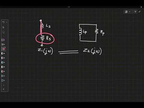
SSCD IIT Kanpur
EE698G lec22: Oscillators-III (LC oscillators)
EE698G (2026): Phase and Frequency Synthesis

SSCD IIT Kanpur
EE698G lec21: Oscillators-II
EE698G (2026): Phase and Frequency Synthesis

SSCD IIT Kanpur
EE698G lec20: Phase noise- III, Introduction to oscillators
EE698G (2026): Phase and Frequency Synthesis

SSCD IIT Kanpur
EE698G lec19: Phase noise, jitter - II
EE698G (2026): Phase and Frequency Synthesis

SSCD IIT Kanpur
EE698G lec18: Phase noise, jitter - I
EE698G (2026): Phase and Frequency Synthesis

SSCD IIT Kanpur
EE698G lec17: DLL applications, introduction to noise
EE698G (2026): Phase and Frequency Synthesis

SSCD IIT Kanpur
EE698G lec16: Discrete-time small-signal phase-domain model for the DLL
EE698G (2026): Phase and Frequency Synthesis

SSCD IIT Kanpur
EE698G lec15: DLL transfer functions
EE698G (2026): Phase and Frequency Synthesis

SSCD IIT Kanpur
EE698G lec14: Small-signal phase domain model of a DLL
EE698G (2026): Phase and Frequency Synthesis
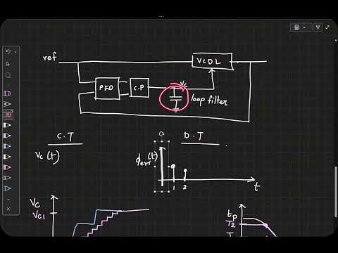
SSCD IIT Kanpur
EE698G 2026 lec13(2): Modelling the DLL for analysis
EE698G (2026): Phase and Frequency Synthesis

SSCD IIT Kanpur
EE698G lec13(1): Mismatches in charge pump, VCDL
EE698G (2026): Phase and Frequency Synthesis

SSCD IIT Kanpur
EE698G lec12: Charge pump implementation - II
EE698G (2026): Phase and Frequency Synthesis

SSCD IIT Kanpur
EE698G lec11: Static phase offset in DLL, charge pump implementation-I
EE698G (2026): Phase and Frequency Synthesis

SSCD IIT Kanpur
EE698G lec10: Locking non-idealities in a DLL
EE698G (2026): Phase and Frequency Synthesis

SSCD IIT Kanpur
EE698G lec9: Locking in a DLL
EE698G (2026): Phase and Frequency Synthesis

SSCD IIT Kanpur
EE698G lec8: Phase detectors - III, charge pump
EE698G (2026): Phase and Frequency Synthesis

SSCD IIT Kanpur
EE698G lec7: Phase detectors - II
EE698G (2026): Phase and Frequency Synthesis

SSCD IIT Kanpur
EE698G lec6: Phase detectors - I
EE698G (2026): Phase and Frequency Synthesis

SSCD IIT Kanpur
EE698G lec5: Voltage-controlled delay lines - II
EE698G (2026): Phase and Frequency Synthesis

SSCD IIT Kanpur
EE698G lec4: Introduction to delay-locked loop, VCDL
EE698G (2026): Phase and Frequency Synthesis

SSCD IIT Kanpur
EE698G lec3: TDC, PVT variation, stabilizing the delay
EE698G (2026): Phase and Frequency Synthesis

SSCD IIT Kanpur
EE698G lec1(4): True time delay vs delaying the edges
EE698G (2026): Phase and Frequency Synthesis
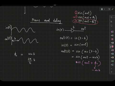
SSCD IIT Kanpur
EE698G lec1(3): Relationship between phase and delay
EE698G (2026): Phase and Frequency Synthesis

SSCD IIT Kanpur
EE698G lec1(2): Relationship between phase and frequency
EE698G (2026): Phase and Frequency Synthesis

SSCD IIT Kanpur
EE698G lec1: Introduction - clock/delay requirements in IC design
EE698G (2026): Phase and Frequency Synthesis

SSCD IIT Kanpur
Lecture 1: Introduction
EE698G: Circuit design for frequency and phase synthesis (2024)

SSCD IIT Kanpur
Lecture 3: Delay-locked loop, tunable delay line
EE698G: Circuit design for frequency and phase synthesis (2024)
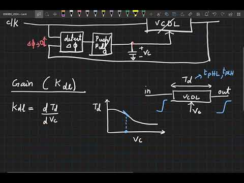
SSCD IIT Kanpur
Lecture 4: Delay tuning using varactors, phase detector
EE698G: Circuit design for frequency and phase synthesis (2024)

SSCD IIT Kanpur
Lecture 5: Phase detectors -II
EE698G: Circuit design for frequency and phase synthesis (2024)

SSCD IIT Kanpur
Lecture 6: Phase detectors - III
EE698G: Circuit design for frequency and phase synthesis (2024)

SSCD IIT Kanpur
Lecture 7: Locking in a DLL
EE698G: Circuit design for frequency and phase synthesis (2024)

SSCD IIT Kanpur
Lecture 8: Locking nonidealities in a DLL
EE698G: Circuit design for frequency and phase synthesis (2024)

SSCD IIT Kanpur
Lecture 10: Charge pumps - II
EE698G: Circuit design for frequency and phase synthesis (2024)

SSCD IIT Kanpur
Lecture 11: Charge pumps - III, transistor mismatches, modelling a DLL
EE698G: Circuit design for frequency and phase synthesis (2024)

SSCD IIT Kanpur
Lecture 12: Small signal phase domain model of the DLL - I
EE698G: Circuit design for frequency and phase synthesis (2024)

SSCD IIT Kanpur
Lecture-13: S-domain model analysis for DLL, Discrete time modeling of DLL
EE698G: Circuit design for frequency and phase synthesis (2024)

SSCD IIT Kanpur
Lecture 14: Discrete time DLL model, Type-II DLL, DLL applications
EE698G: Circuit design for frequency and phase synthesis (2024)

SSCD IIT Kanpur
Lecture 15: Noise, PSD, thermal and flicker noise
EE698G: Circuit design for frequency and phase synthesis (2024)
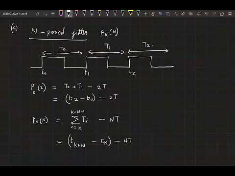
SSCD IIT Kanpur
Lecture 16: Jitter definitions, jitter characterizations
EE698G: Circuit design for frequency and phase synthesis (2024)

SSCD IIT Kanpur
Lecture 17: Relationship between phase noise and jitter
EE698G: Circuit design for frequency and phase synthesis (2024)

SSCD IIT Kanpur
Lecture 18: Phase noise/jitter analysis in VCO, inverter and delay line
EE698G: Circuit design for frequency and phase synthesis (2024)

SSCD IIT Kanpur
Lecture 19: Jitter in delay line vs ring oscillator; Oscillators-I
EE698G: Circuit design for frequency and phase synthesis (2024)
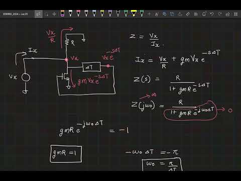
SSCD IIT Kanpur
Lecture 20: Oscillators - II
EE698G: Circuit design for frequency and phase synthesis (2024)

SSCD IIT Kanpur
Lecture 21: Oscillators--III
EE698G: Circuit design for frequency and phase synthesis (2024)
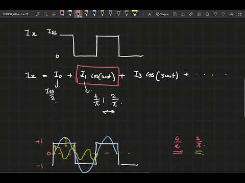
SSCD IIT Kanpur
Lecture 22: Oscillators-IV
EE698G: Circuit design for frequency and phase synthesis (2024)

SSCD IIT Kanpur
Lecture 23: Oscillators-V
EE698G: Circuit design for frequency and phase synthesis (2024)

SSCD IIT Kanpur
Lecture 24: Design of a ring oscillator
EE698G: Circuit design for frequency and phase synthesis (2024)

SSCD IIT Kanpur
Lecture 25: Design of ring oscillator-II, Introduction to PLL
EE698G: Circuit design for frequency and phase synthesis (2024)

SSCD IIT Kanpur
Lecture 26: Phase-locked loop - II
EE698G: Circuit design for frequency and phase synthesis (2024)

SSCD IIT Kanpur
Lecture 27: Phase-locked loop - III
EE698G: Circuit design for frequency and phase synthesis (2024)

SSCD IIT Kanpur
Lecture 1: Sampling, anti-alias filter, oversampling, reconstruction; Into to Quantization
EE698I: Mixed-signal IC design (2023)

SSCD IIT Kanpur
Lecture 2: Measuring SQNR; Refresher on Fourier analysis; Evolution of discrete Fourier transform
EE698I: Mixed-signal IC design (2023)

SSCD IIT Kanpur
Lecture 3: DFT of sinusoid; Spectral leakage; Need for windowing; Choice of input freq. to test ADC
EE698I: Mixed-signal IC design (2023)

SSCD IIT Kanpur
Lecture 4: Differential & Integral non-linearity (DNL, INL); MOS as switch; Effect of finite ON res.
EE698I: Mixed-signal IC design (2023)
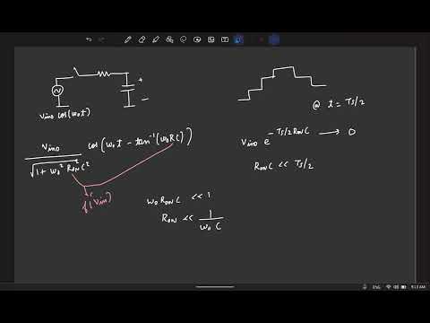
SSCD IIT Kanpur
Lecture 5: Switch non-linearity; Gate bootstrapped switch; Thermal noise
EE698I: Mixed-signal IC design (2023)

SSCD IIT Kanpur
Lecture 6 (pt 1): Charge injection, bottom plate sampling, deriving the switched-capacitor amplifier
EE698I: Mixed-signal IC design (2023)

SSCD IIT Kanpur
Lecture 6 (pt 2): Analyzing switched capacitor ckts using KCL & understanding charge conservation
EE698I: Mixed-signal IC design (2023)

SSCD IIT Kanpur
Lecture 7: Charge conservation: more examples; Switched capacitor integrators (delayed & delay-free)
EE698I: Mixed-signal IC design (2023)

SSCD IIT Kanpur
Lecture 8: Correlated double sampling (CDS); Correlated level shifting (CLS); gain error & offset
EE698I: Mixed-signal IC design (2023)

SSCD IIT Kanpur
Lecture 9 (pt. 1): Using an OTA vs an opamp in switched capacitor ckts; Settling & slewing with OTA
EE698I: Mixed-signal IC design (2023)

SSCD IIT Kanpur
Lecture 9 (pt. 2):Noise in switched cap(SC) ckts with OTA; Mean-squared noise in SC ckts without OTA
EE698I: Mixed-signal IC design (2023)

SSCD IIT Kanpur
Lecture 10: Deriving the StrongARM latch; Introduction to Flash ADC
EE698I: Mixed-signal IC design (2023)

SSCD IIT Kanpur
Problem discussion; Deriving the Floating inverter amplifier (FIA); Dynamic amplifiers for SC ckts.
EE698I: Mixed-signal IC design (2023)

SSCD IIT Kanpur
Lecture 11: Flash ADC: Ref. subtraction; Dynamic premp; Offset calibration; offset as ref. for flash
EE698I: Mixed-signal IC design (2023)

SSCD IIT Kanpur
Lecture 12(1): Flash ADC summary; Common-mode rejection in floating inverter amp FIA & integ dyn amp
EE698I: Mixed-signal IC design (2023)

SSCD IIT Kanpur
Lecture 12(2): Interpolating Flash ADC; Time interpolation in flash ADC; Some examples in literature
EE698I: Mixed-signal IC design (2023)

SSCD IIT Kanpur
Lecture 13: Time-interleaved ADCs; Offset, gain and timing mismatches
EE698I: Mixed-signal IC design (2023)

SSCD IIT Kanpur
Lecture 14: SAR ADC; Capacitive DAC switching schemes; Monotonic switching; Energy efficiency
EE698I: Mixed-signal IC design (2023)

SSCD IIT Kanpur
Lecture 15 (1): Asynchronous SAR ADC; Implementing the asynchronous logic
EE698I: Mixed-signal IC design (2023)

SSCD IIT Kanpur
Lecture 15 (2): SAR ADC: Redundancy to tackle DAC settling; Condition for redundancy; Example calc.
EE698I: Mixed-signal IC design (2023)
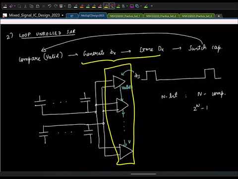
SSCD IIT Kanpur
Lecture 16: SAR ADC: Loop unrolled SAR; Split C-DAC; Digital calibration; Buffer embedded SAR
EE698I: Mixed-signal IC design (2023)

SSCD IIT Kanpur
Lecture 17: Pipelined ADC; Redundancy to tackle comparator offset; 1.5-bit (M+0.5) bit stage;
EE698I: Mixed-signal IC design (2023)

SSCD IIT Kanpur
Lecture 18: Pipelined-Flash: Multiplying DAC(MDAC) non-idealities: gain error, non-lin; DAC non-lin.
EE698I: Mixed-signal IC design (2023)

SSCD IIT Kanpur
Lecture 19(1): Pipelined ADC: Digital calibration: Using a PN dither & correlation; Gradient descent
EE698I: Mixed-signal IC design (2023)

SSCD IIT Kanpur
Lecture 19(2): Split ADC structure for digital calibration of pipelined ADCs & time-interleaved ADCs
EE698I: Mixed-signal IC design (2023)

SSCD IIT Kanpur
Lecture 19(3): Pipelined ADC: Design choices and trade-offs
EE698I: Mixed-signal IC design (2023)
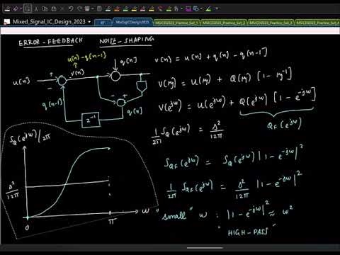
SSCD IIT Kanpur
Lecture 20: Noise-shaping ADC: Deriving the Error-feedback structure; Intro to delta-sigma modulator
EE698I: Mixed-signal IC design (2023)

SSCD IIT Kanpur
Lecture 21: Delta-sigma modulator: Higher order NTF; Maximum stable amplitude (MSA); Controlling OBG
EE698I: Mixed-signal IC design (2023)
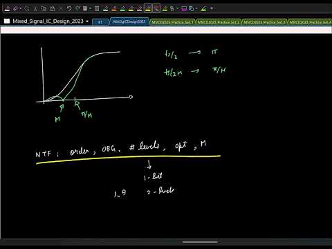
SSCD IIT Kanpur
Lecture 22 (1): Delta-sigma modulator: system-level design; simple design example in MATLAB
EE698I: Mixed-signal IC design (2023)

SSCD IIT Kanpur
Lecture 22 (pt. 2): Intuition behind the loop filter coefficients; Circuit implementation of MOD1
EE698I: Mixed-signal IC design (2023)

SSCD IIT Kanpur
Lecture 23: Switched-capacitor loop filter; DAC mismatch; Data weighted averaging (DWA)
EE698I: Mixed-signal IC design (2023)

SSCD IIT Kanpur
Lecture 24 (1): Motivation for Continuous time delta-sigma modulator (CTDSM): Implicit anti-aliasing
EE698I: Mixed-signal IC design (2023)

SSCD IIT Kanpur
Lecture 24 (2): VCO-based ADC: basic introduction
EE698I: Mixed-signal IC design (2023)

SSCD IIT Kanpur
Lecture 24 (3): Schrier Figure of Merit (FoM) for ADCs
EE698I: Mixed-signal IC design (2023)

SSCD IIT Kanpur
Lecture 19(2): Digital calibration with PN dither based correlation: Gradient descent & LMS
EE698I: Mixed-signal IC design (2024)

SSCD IIT Kanpur
Lecture 19(1): Pipelined ADC: Thermal noise
EE698I: Mixed-signal IC design (2024)

SSCD IIT Kanpur
Lecture 18(3): Pipelined ADC: M-DAC gain error & DAC mismatch: Digital calibration to tackle them
EE698I: Mixed-signal IC design (2024)

SSCD IIT Kanpur
Lecture 18(2): Pipelined Flash ADC: Circuit implementation of the multiplying-DAC (M-DAC)
EE698I: Mixed-signal IC design (2024)

SSCD IIT Kanpur
Lecture 18(1): Pipelined ADC: Redundancy to tackle sub-ADC error; Deriving 1.5 bit & M+0.5 bit stage
EE698I: Mixed-signal IC design (2024)

SSCD IIT Kanpur
Lecture 17(3): Introduction to multi-step & Pipelined ADCs
EE698I: Mixed-signal IC design (2024)

SSCD IIT Kanpur
Lecture 17(2): SAR ADC: Effect of capacitor mismatch: Understanding why digital calibration works
EE698I: Mixed-signal IC design (2024)

SSCD IIT Kanpur
Lecture 17(1): SAR ADC: Split C-DAC technique for reducing the total capacitance
EE698I: Mixed-signal IC design (2024)

SSCD IIT Kanpur
Lecture 16(2): Redundancy to solve incomplete DAC settling; Deriving condition for redundancy & eg.,
EE698I: Mixed-signal IC design (2024)

SSCD IIT Kanpur
Lecture 16(1): Asynchronous SAR ADC: Understanding how to implement a self-timed asynchronous SAR
EE698I: Mixed-signal IC design (2024)

SSCD IIT Kanpur
Lecture 15: SAR ADC; Deriving the capacitive DAC switching schemes & the monotonic switching scheme
EE698I: Mixed-signal IC design (2024)

SSCD IIT Kanpur
Lecture 14: Time-interleaved ADCs; Gain, timing & offset mismatch; Calibration to correct mismatches
EE698I: Mixed-signal IC design (2024)

SSCD IIT Kanpur
Lecture 13: Interpolation in Flash ADC: Voltage & Time based interpolation
EE698I: Mixed-signal IC design (2024)

SSCD IIT Kanpur
Lecture 12(2): Latch offset: Using dynamic pre-amplifier & Calibration to reduce offset
EE698I: Mixed-signal IC design (2024)

SSCD IIT Kanpur
Lecture 12(1): Flash ADC: single-ended & differential; Reference subtraction in voltage & current
EE698I: Mixed-signal IC design (2024)

SSCD IIT Kanpur
Lecture 11: Deriving the StrongARM latch
EE698I: Mixed-signal IC design (2024)

SSCD IIT Kanpur
Lecture 9(2): Miscellanea on switched-capacitors
EE698I: Mixed-signal IC design (2024)

SSCD IIT Kanpur
Lecture 9(1): Correlated double-sampling (CDS) & correlated level-shifting (CLS)
EE698I: Mixed-signal IC design (2024)

SSCD IIT Kanpur
Lecture 8(2): N-path filters & passive mixers (brief introduction)
EE698I: Mixed-signal IC design (2024)

SSCD IIT Kanpur
Lecture 8(1): Switched-capacitor integrator (delayed & delay-free)
EE698I: Mixed-signal IC design (2024)

SSCD IIT Kanpur
Lecture 7: Recap; Example problems on solving switched-capacitor circuits using charge conservation
EE698I: Mixed-signal IC design (2024)

SSCD IIT Kanpur
Lecture 6(3): Understanding charge-conservation in switched-capacitor circuits from KCL
EE698I: Mixed-signal IC design (2024)

SSCD IIT Kanpur
Lecture 6(2): Deriving the switched-capacitor amplifier
EE698I: Mixed-signal IC design (2024)

SSCD IIT Kanpur
Lecture 6(1): Non-linearity from signal-dependent charge injection; Bottom-plate sampling to rescue
EE698I: Mixed-signal IC design (2024)

SSCD IIT Kanpur
Lecture 5(3): Thermal noise of switch; Variance & PSD of sampled noise in a track & hold
EE698I: Mixed-signal IC design (2024)

SSCD IIT Kanpur
Lecture 5(2): Deriving the gate boostrapped switch
EE698I: Mixed-signal IC design (2024)

SSCD IIT Kanpur
Lecture 5(1): ON resistance of a MOS switch & non-linearity; CMOS/transmission gate switch
EE698I: Mixed-signal IC design (2024)

SSCD IIT Kanpur
Lecture 4(3): Sampling switch; Effect of finite ON resistance for dc & varying signals; nMOS switch
EE698I: Mixed-signal IC design (2024)

SSCD IIT Kanpur
Lecture 4(2): Static non-linearity of an ADC: Differential & Integral non-linearity (DNL & INL)
EE698I: Mixed-signal IC design (2024)

SSCD IIT Kanpur
Lecture 4(1): Example calculations from ADC spectrum; Aliasing of harmonics
EE698I: Mixed-signal IC design (2024)

SSCD IIT Kanpur
Lecture 3(2): Windowing to reduce spectral leakage; Choosing the right input frequency to test ADC
EE698I: Mixed-signal IC design (2024)

SSCD IIT Kanpur
Lecture 3(1): Recap; DFT of a sinusoid; Signal on a bin; Signal not on a bin: Spectral leakage
EE698I: Mixed-signal IC design (2024)

SSCD IIT Kanpur
Lecture 2(3): Deriving the discrete Fourier transform (DFT); Measuring SQNR
EE698I: Mixed-signal IC design (2024)
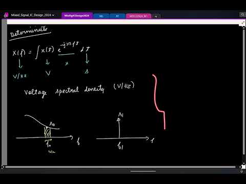
SSCD IIT Kanpur
Lecture 2(2): Measuring SQNR: Recap of spectral analysis; Voltage & power spectral density (PSD)
EE698I: Mixed-signal IC design (2024)

SSCD IIT Kanpur
Lecture 2(1): Quantization; Signal-to-quantization noise ratio (SQNR); Effective no. bits (ENOB)
EE698I: Mixed-signal IC design (2024)

SSCD IIT Kanpur
Lecture 1: Sampling: aliasing, anti-alias filter, oversampling; Signal reconstruction from samples
EE698I: Mixed-signal IC design (2024)

SSCD IIT Kanpur
Lecture 1: Introduction to the course
EE698L: RFIC Design

SSCD IIT Kanpur
Lecture 2: Introduction to basic Transceiver architecture (contd..)
EE698L: RFIC Design

SSCD IIT Kanpur
Lecture 3a: Why is 50ohm the impedance of choice?
EE698L: RFIC Design

SSCD IIT Kanpur
Lecture 3b: Intro to RF chain contd.. (Linear PA)
EE698L: RFIC Design

SSCD IIT Kanpur
Lecture 3c: Intro to RF chain contd.. (Switching PA)
EE698L: RFIC Design

SSCD IIT Kanpur
Lecture 4: Intro to RF chain contd.. (Requirement of filtering in Receiver) need for matching.
EE698L: RFIC Design

SSCD IIT Kanpur
Lecture 5: Introduction to RF chain contd.. (Effect of transmission lines; need for matching)
EE698L: RFIC Design

SSCD IIT Kanpur
Lecture 6: Intro to RF chain contd... A ten-thousand feet overview on clocking, VCO and PLL.
EE698L: RFIC Design

SSCD IIT Kanpur
Lecture 7: LO leakage in mixers and its impact on the overall Rx
EE698L: RFIC Design

SSCD IIT Kanpur
Lecture 8: Issues with direct-downconversion Rx and evolution of super-heterodyne Rx
EE698L: RFIC Design

SSCD IIT Kanpur
Lecture 9: Introduction to thermal noise
EE698L: RFIC Design

SSCD IIT Kanpur
Lecture 10: Noise in cascaded systems; Input referred noise
EE698L: RFIC Design

SSCD IIT Kanpur
Lecture 11: Input referred noise: Noise Figure
EE698L: RFIC Design

SSCD IIT Kanpur
Lecture 12: Sensitivity of an Rx; Optimizing source resistance to minimize NF
EE698L: RFIC Design
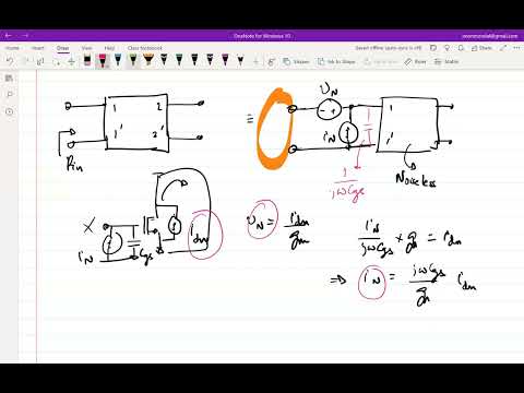
SSCD IIT Kanpur
Lecture 13: NF optimization for generic two-port network; Introduction to matching networks
EE698L: RFIC Design

SSCD IIT Kanpur
Lecture 14: Matching network contd..
EE698L: RFIC Design

SSCD IIT Kanpur
Lecture 15: Losses in matching network- Multi-stage matching
EE698L: RFIC Design

SSCD IIT Kanpur
Lecture 16: Need for scattering parameters
EE698L: RFIC Design

SSCD IIT Kanpur
Lecture 17: Measures of distortion in RF systems.
EE698L: RFIC Design

SSCD IIT Kanpur
Lecture 18a: Techniques to mitigate distortion.
EE698L: RFIC Design

SSCD IIT Kanpur
Lecture 18b: Narrowband LNA design
EE698L: RFIC Design

SSCD IIT Kanpur
Lecture 19: LNA with inductive degeneration; design considerations
EE698L: RFIC Design

SSCD IIT Kanpur
Lecture 20: Mixers- Single balanced and double-balanced
EE698L: RFIC Design

SSCD IIT Kanpur
Lecture 21: Image rejection in super-heterodyne Rx
EE698L: RFIC Design
SSCD IIT Kanpur
Untitled video
EE698L: RFIC Design

SSCD IIT Kanpur
Lecture 23: Introduction to power amplifiers
EE698L: RFIC Design
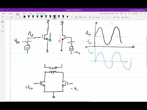
SSCD IIT Kanpur
Lecture 24: Class B and AB power amplifier; Power mixer
EE698L: RFIC Design
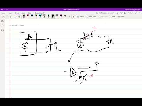
SSCD IIT Kanpur
Lecture 25: PA linearization techniques; Switching PA
EE698L: RFIC Design

Dr. Shubham Sahay
Lecture - 1 Memory organization
EE698P: Memory Technology and Neuromorphic Computing

Dr. Shubham Sahay
Lecture - 2.1 Segregation of Memory Devices
EE698P: Memory Technology and Neuromorphic Computing
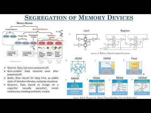
Dr. Shubham Sahay
Lecture - 2.2 Memory arrays and characteristics
EE698P: Memory Technology and Neuromorphic Computing

Dr. Shubham Sahay
Lecture - 3 Memory Market
EE698P: Memory Technology and Neuromorphic Computing

Dr. Shubham Sahay
Lecture 4 - Memory Array Architecture
EE698P: Memory Technology and Neuromorphic Computing

Dr. Shubham Sahay
Lecture 5 - Read and Write operation in SRAM
EE698P: Memory Technology and Neuromorphic Computing

Dr. Shubham Sahay
Lecture 6 - Read/Write conflict and Other SRAM cells
EE698P: Memory Technology and Neuromorphic Computing

Dr. Shubham Sahay
Lecture 8 - SRAM peripheral circuitry
EE698P: Memory Technology and Neuromorphic Computing

Dr. Shubham Sahay
Lecture 7 - Noise Margin in SRAM
EE698P: Memory Technology and Neuromorphic Computing

Dr. Shubham Sahay
Lecture 9 - Introduction to DRAMs
EE698P: Memory Technology and Neuromorphic Computing

Dr. Shubham Sahay
Lecture 10 - Single-ended sensing and organization of DRAM
EE698P: Memory Technology and Neuromorphic Computing

Dr. Shubham Sahay
Lecture 11 - Introduction to Flash Memory
EE698P: Memory Technology and Neuromorphic Computing

Dr. Shubham Sahay
Lecture 12 - NAND and NOR Flash memory
EE698P: Memory Technology and Neuromorphic Computing

Dr. Shubham Sahay
Lecture 13 - Reliability of Flash memory
EE698P: Memory Technology and Neuromorphic Computing

Dr. Shubham Sahay
Lecture 14 - Multi-bit Capability in Flash memory
EE698P: Memory Technology and Neuromorphic Computing

Dr. Shubham Sahay
Lecture 15 - Organization of NAND flash memory
EE698P: Memory Technology and Neuromorphic Computing

Dr. Shubham Sahay
Lecture 17 - 3D Vertical Channel Flash memory
EE698P: Memory Technology and Neuromorphic Computing

Dr. Shubham Sahay
Lecture 18 - Fabrication of BiCS Flash cell
EE698P: Memory Technology and Neuromorphic Computing

Dr. Shubham Sahay
Lecture 16 - Charge-Trap Flash memory
EE698P: Memory Technology and Neuromorphic Computing

Dr. Shubham Sahay
Lecture 19 - Advance 3D NAND Flash configurations
EE698P: Memory Technology and Neuromorphic Computing

Dr. Shubham Sahay
Lecture 20 - Issues with 3D NAND flash memory
EE698P: Memory Technology and Neuromorphic Computing

Dr. Shubham Sahay
Lecture 21 - Phase-change Materials
EE698P: Memory Technology and Neuromorphic Computing

Dr. Shubham Sahay
Lecture 22 - Phase-change Memories
EE698P: Memory Technology and Neuromorphic Computing

Dr. Shubham Sahay
Lecture 23 - Resistive RAMs
EE698P: Memory Technology and Neuromorphic Computing

Dr. Shubham Sahay
Lecture 24 - RRAM characteristics
EE698P: Memory Technology and Neuromorphic Computing

Dr. Shubham Sahay
Lecture 25 - Conductive Bridge RAM/Programmable Metallization Cell
EE698P: Memory Technology and Neuromorphic Computing

Dr. Shubham Sahay
Lecture 26 - Ferroelectric Memories
EE698P: Memory Technology and Neuromorphic Computing

Dr. Shubham Sahay
Lecture 27 - Physical Unclonable functions
EE698P: Memory Technology and Neuromorphic Computing

Dr. Shubham Sahay
Lecture 28 - Random Number Generators
EE698P: Memory Technology and Neuromorphic Computing
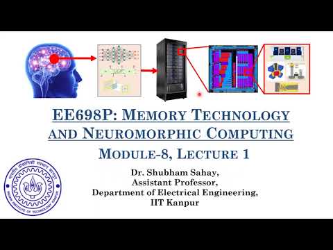
Dr. Shubham Sahay
Lecture 29 - Neuromorphic Computing and Neurobiology
EE698P: Memory Technology and Neuromorphic Computing

Dr. Shubham Sahay
Lecture 30 - Synapses and their learning rule
EE698P: Memory Technology and Neuromorphic Computing
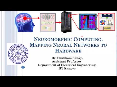
Dr. Shubham Sahay
Lecture 31 - Mapping Neural Networks to Hardware
EE698P: Memory Technology and Neuromorphic Computing

SSCD IIT Kanpur
Lecture 23: Inter-reciprocity in LPTV network - Integrated noise in switched RC circuit
EE698W: Analog Circuits for Signal Processing (2025)

SSCD IIT Kanpur
Lecture 22: N-path operation contd..
EE698W: Analog Circuits for Signal Processing (2025)

SSCD IIT Kanpur
Lecture 21: Introduction to N-path filters
EE698W: Analog Circuits for Signal Processing (2025)

SSCD IIT Kanpur
Lecture 20: Finding envelope of an LPTV network with large time-constant using sinusoidal inputs
EE698W: Analog Circuits for Signal Processing (2025)

SSCD IIT Kanpur
Lecture 19: Switched RC frequency response contd..
EE698W: Analog Circuits for Signal Processing (2025)

SSCD IIT Kanpur
Lecture 18: Analysis of an LPTV network through the example of a switched RC circuit.
EE698W: Analog Circuits for Signal Processing (2025)

SSCD IIT Kanpur
Lecture 16: Analysis of an LTV system through the example of an RC network
EE698W: Analog Circuits for Signal Processing (2025)

SSCD IIT Kanpur
Lecture 15: Impulse response in time-varying network
EE698W: Analog Circuits for Signal Processing (2025)

SSCD IIT Kanpur
Lecture 13: Distortion analysis - current injection method
EE698W: Analog Circuits for Signal Processing (2025)

SSCD IIT Kanpur
Lecture 12: Distortion in analog circuits
EE698W: Analog Circuits for Signal Processing (2025)

SSCD IIT Kanpur
Lecture 11: Noise in cascaded systems; Integrated noise
EE698W: Analog Circuits for Signal Processing (2025)

SSCD IIT Kanpur
Lecture 10: Nyquist noise theorem, input referred noise
EE698W: Analog Circuits for Signal Processing (2025)

SSCD IIT Kanpur
Lecture 9: Noisy network analysis
EE698W: Analog Circuits for Signal Processing (2025)

SSCD IIT Kanpur
Lecture 8: Inter-reciprocity contd.. Introduction to thermal noise.
EE698W: Analog Circuits for Signal Processing (2025)
SSCD IIT Kanpur
Lecture 7: Inter-reciprocity
EE698W: Analog Circuits for Signal Processing (2025)

SSCD IIT Kanpur
Lecture 6: Introduction to Tellegen's theorem, and proof of reciprocity
EE698W: Analog Circuits for Signal Processing (2025)

SSCD IIT Kanpur
Lecture 5: ZVT method with inductors; Estimation of number of poles and zeros
EE698W: Analog Circuits for Signal Processing (2025)

SSCD IIT Kanpur
Lecture 4: Evaluating polynomial coefficients contd..
EE698W: Analog Circuits for Signal Processing (2025)

SSCD IIT Kanpur
Lecture 3: Evaluating polynomial coefficients in a transfer function
EE698W: Analog Circuits for Signal Processing (2025)

SSCD IIT Kanpur
Lecture 2: Transfer function and its relation to time-domain signal processing
EE698W: Analog Circuits for Signal Processing (2025)

SSCD IIT Kanpur
Lecture 1: Introduction: LTI systems
EE698W: Analog Circuits for Signal Processing (2025)

SSCD IIT Kanpur
Lecture 25: Impedance and admittance in LPTV systems - Concluding remarks
EE698W: Analog Circuits for Signal Processing (2025)

SSCD IIT Kanpur
Lec 39: FSMs in processors: branch predictor FSM to avoid pipeline flush; concluding remarks
ESC 201: Introduction to electronics (2026)
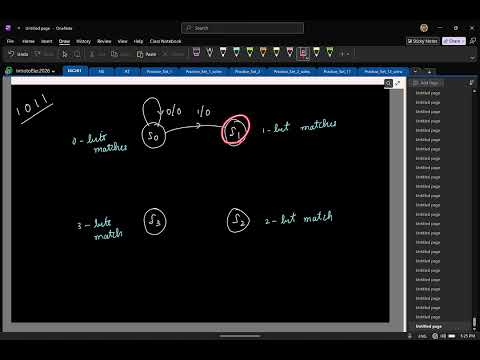
SSCD IIT Kanpur
Lec 38: Mealy FSM design: Sequence detectors, counting odd/even
ESC 201: Introduction to electronics (2026)
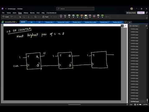
SSCD IIT Kanpur
Lec 37: Finite state machine (FSM) design example: Synchronous counters
ESC 201: Introduction to electronics (2026)

SSCD IIT Kanpur
Lec 36: Finite state machines (FSM): Practice problem discussion
ESC 201: Introduction to electronics (2026)

SSCD IIT Kanpur
Lec 35: Designing asynchronous/ripple-carry counters
ESC 201: Introduction to electronics (2026)

SSCD IIT Kanpur
Lec 34: Example calculation: Finding state transition graphs & output sequence; Intro to counters
ESC 201: Introduction to electronics (2026)

SSCD IIT Kanpur
Lec 33: Finite state machine (FSM) Analyzing an FSM: state transition table & state transition graph
ESC 201: Introduction to electronics (2026)

SSCD IIT Kanpur
Lec 32: The D flip-flop & the JK flip-flop
ESC 201: Introduction to electronics (2026)

SSCD IIT Kanpur
Lec 31: JK latch, T latch and D latch
ESC 201: Introduction to electronics (2026)
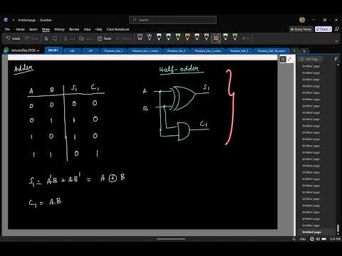
SSCD IIT Kanpur
Lec 30: The Set-Reset (SR) latch
ESC 201: Introduction to electronics (2026)

SSCD IIT Kanpur
Lec 29: Mux (recap); Decoders for realizing logic function; Building a ROM using decoders & OR gates
ESC 201: Introduction to electronics (2026)

SSCD IIT Kanpur
Lec 28: Four-variable K-Map; Multiplexers to realize a logic function
ESC 201: Introduction to electronics (2026)
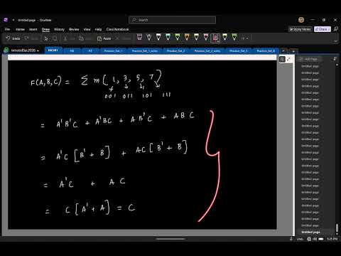
SSCD IIT Kanpur
Lec 27: Karnaugh map (K-map) for logic minimization
ESC 201: Introduction to electronics (2026)

SSCD IIT Kanpur
Lec 26: Logic realization using SOP & POS forms; Logic minimization using boolean algebra
ESC 201: Introduction to electronics (2026)

SSCD IIT Kanpur
Lec 25: Logic gates; NOT gate with switches & transistors; Voltage transfer characteristic (VTC)
ESC 201: Introduction to electronics (2026)

SSCD IIT Kanpur
Lec 24: Understanding 2s complement; 2s complement arithmetic
ESC 201: Introduction to electronics (2026)

SSCD IIT Kanpur
Lec 23(1): Conversion between number systems (integer & fractional parts)
ESC 201: Introduction to electronics (2026)

SSCD IIT Kanpur
Lec 23(2): Deriving the idea of 10s complement
ESC 201: Introduction to electronics (2026)

SSCD IIT Kanpur
Lec 22: Positional number systems: Binary, Octal, Hexadecimal; Noise tolerance in binary digital sig
ESC 201: Introduction to electronics (2026)

SSCD IIT Kanpur
Lec 21: Opamp-based RC low-pass filter; Opamp as comparator; Need for hysteresis; Schmitt trigger
ESC 201: Introduction to electronics (2026)

SSCD IIT Kanpur
Lec 20: Opamp based sensor interface circuits example; Opamp circuits with capacitors
ESC 201: Introduction to electronics (2026)

SSCD IIT Kanpur
Lec 19: Finding opamp signs for negative feedback; Using voltage buffer & inverting amplifier
ESC 201: Introduction to electronics (2026)
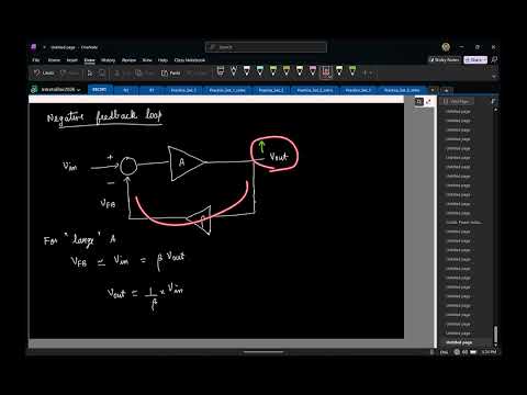
SSCD IIT Kanpur
Lec 18: Examples of negative feedback: Introducing opamp; Non-inverting amplifier using opamp
ESC 201: Introduction to electronics (2026)

SSCD IIT Kanpur
Lec 16: Phasor representation; Thevenin's theorem with capacitors & inductors; Intro to AC power
ESC 201: Introduction to electronics (2026)

SSCD IIT Kanpur
Lec 15: 2nd order circuits: Series RLC: Resonance, bandwidth, oscillations
ESC 201: Introduction to electronics (2026)

SSCD IIT Kanpur
Lec 14: Bode plot: Bode approximation for the magnitude plot
ESC 201: Introduction to electronics (2026)

SSCD IIT Kanpur
Lec 13: Low-pass filter example demo; Intro to Lissajous figures
ESC 201: Introduction to electronics (2026)

SSCD IIT Kanpur
Lec 12: Impedance & frequency response; 1st-order RC & RL circuits as filters
ESC 201: Introduction to electronics (2026)

SSCD IIT Kanpur
Lec 11(2): Sinusoidal steady-state response of first-order circuits
ESC 201: Introduction to electronics (2026)

SSCD IIT Kanpur
Lec 11(1): First-order RL circuits; Example calculations
ESC 201: Introduction to electronics (2026)

SSCD IIT Kanpur
Lec 10: RC circuits with two capacitors: Finding initial value, final value, time constant: examples
ESC 201: Introduction to electronics (2026)

SSCD IIT Kanpur
Lec 9: First-order RC circuits: Natural response & forced response
ESC 201: Introduction to electronics (2026)

SSCD IIT Kanpur
Lec 8: Capacitors: RC circuits; Can a capacitor voltage change instantly? Capacitor blocks DC?
ESC 201: Introduction to electronics (2026)

SSCD IIT Kanpur
Lec 7: Source transformation; Thevenin & Norton theorem
ESC 201: Introduction to electronics (2026)

SSCD IIT Kanpur
Lec 6: Superposition principle in linear circuits
ESC 201: Introduction to electronics (2026)

SSCD IIT Kanpur
Lec 5: Current division; Voltage/current sources in series & parallel; Introducing dependent sources
ESC 201: Introduction to electronics (2026)
SSCD IIT Kanpur
Lec4(2): Brief on oscilloscope trigger settings
ESC 201: Introduction to electronics (2026)

SSCD IIT Kanpur
Lec 4: Tricks to solve circuits fast: series & parallel connections; Voltage divider
ESC 201: Introduction to electronics (2026)

SSCD IIT Kanpur
Lec 3: Nodal analysis with voltage sources; Using supernode; Mesh analysis using KVL
ESC 201: Introduction to electronics (2026)

SSCD IIT Kanpur
Lec 2(2): Kirchhoff's current law (KCL) & Nodal analysis
ESC 201: Introduction to electronics (2026)

SSCD IIT Kanpur
Lec 2: Power dissipation; Recap of resistor, inductor & capacitor; Are capacitors active devices?
ESC 201: Introduction to electronics (2026)

SSCD IIT Kanpur
Lec 1: Why electronics? Defining energy, power; voltage & current sources; active vs passive devices
ESC 201: Introduction to electronics (2026)

SSCD IIT Kanpur
Chip design at SSCD IITK
Members of SSCD-IITK

SSCD IIT Kanpur
Chip talk @ SSCD: Aasif introduces his work on wideband delay-lines
Members of SSCD-IITK

SSCD IIT Kanpur
Intro to noise-shaping ADCs: Delta-sigma modulators, error-feedback noise-shaping & VCO-based ADCs
Tutorial talks
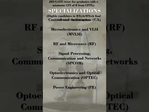
SSCD IIT Kanpur
EE IITK PhD Admissions 2026: Your Research Journey Begins! #sscd #iitk #icdesign
Uploads from SSCD IIT Kanpur

SSCD IIT Kanpur
EE801 (PG seminar course): Do's & Don'ts in a good presentation
Uploads from SSCD IIT Kanpur

SSCD IIT Kanpur
Expansion and compression of analog pulses
Uploads from SSCD IIT Kanpur

SSCD IIT Kanpur
Why are Indians so good at circuit design? 🤔😂
Uploads from SSCD IIT Kanpur

SSCD IIT Kanpur
"Chip" design: then vs. now! 😂
Uploads from SSCD IIT Kanpur

SSCD IIT Kanpur
An Automatic Leakage Compensation Technique for Capacitively Coupled Class-AB Operational Amplifiers
Uploads from SSCD IIT Kanpur

SSCD IIT Kanpur
Lecture 36: Basics of analog layout, and concluding remarks
Uploads from SSCD IIT Kanpur

SSCD IIT Kanpur
Lecture 35: The method of non-linear currents or current injection to analyze weakly non-linear ckts
Uploads from SSCD IIT Kanpur

SSCD IIT Kanpur
Lecture 34: CMOS inv; Class AB stage; Non-linearity in negative feedback
Uploads from SSCD IIT Kanpur

SSCD IIT Kanpur
Lecture 33 (pt. 2): Scaling in analog circuits: Noise/impedance scaling and frequency scaling
Uploads from SSCD IIT Kanpur

SSCD IIT Kanpur
Lecture 33 (pt. 1): Noise & offset in multi-stage amps; Noise & SNR in fully differential circuits
Uploads from SSCD IIT Kanpur

SSCD IIT Kanpur
Lecture 32 (errata): Noise calculation
Uploads from SSCD IIT Kanpur

SSCD IIT Kanpur
Lecture 32: Input ref. noise & offset in 5-transistor OTA, telescopic cascode, folded cascode OTA
Uploads from SSCD IIT Kanpur

SSCD IIT Kanpur
Lecture 31: Input referred noise calc with eg.; Input referred noise of a MOSFET; noise in a cascode
Uploads from SSCD IIT Kanpur

SSCD IIT Kanpur
Lecture 30: Noise in MOSFETs; Input referred noise voltage and current; Noise calc. in CS & CG amp.
Uploads from SSCD IIT Kanpur

SSCD IIT Kanpur
Lecture 29: Mismatch in current mirror; Intro to noise; Power spectral density; Noise in resistors
Uploads from SSCD IIT Kanpur

SSCD IIT Kanpur
Lecture 28: Resistors and capacitors on ICs; Random mismatch; Process variations; Pelgrom's law
Uploads from SSCD IIT Kanpur

SSCD IIT Kanpur
Lecture 27: Long recap; Common-mode rejection with CMFB; Output impedance with negative feedback
Uploads from SSCD IIT Kanpur

SSCD IIT Kanpur
Lecture 26: 2-stage fully-diff. Miller OTA, CMFB choices; fully diff. 2-stage feedforward OTA & CMFB
Uploads from SSCD IIT Kanpur

SSCD IIT Kanpur
Lecture 25: CMFB variants: source follower + res. CMD, MOS-based CMD, replica biasing, etc.
Uploads from SSCD IIT Kanpur

SSCD IIT Kanpur
Lecture 24: Need for common-mode feedback (CMFB); CMFB variants using resistive common-mode detector
Uploads from SSCD IIT Kanpur

SSCD IIT Kanpur
Lecture 23: Motivation for differential signaling; pseudo-differential vs. fully differential ckts.
Uploads from SSCD IIT Kanpur

SSCD IIT Kanpur
Lecture 22: Lookup table based systematic design of analog circuits (gm/Id based design)
Uploads from SSCD IIT Kanpur

SSCD IIT Kanpur
Lecture 21: Feedforward compensation; Comparing Miller and feedforward compensation
Uploads from SSCD IIT Kanpur

SSCD IIT Kanpur
Lecture 20: Midsem quiz discussion; Nested Miller compensation
Uploads from SSCD IIT Kanpur

SSCD IIT Kanpur
Lecture 19 (pt. 1): Two-stage Miler compensated OTA: Design example #2
Uploads from SSCD IIT Kanpur

SSCD IIT Kanpur
Lecture 18: Ahuja compensation; Using the zero cancelling resistor; Miller OTA design example #1
Uploads from SSCD IIT Kanpur

SSCD IIT Kanpur
Lecture 17: Miller OTA: Eliminating RHP zero; source follower (VCVS); zero cancelling resistor
Uploads from SSCD IIT Kanpur

SSCD IIT Kanpur
Lecture 16: 2-stage Miller OTA; design iteration eg., transistor-level schematic; Systematic offset
Uploads from SSCD IIT Kanpur
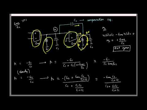
SSCD IIT Kanpur
Lecture 15: Two-stage Miller compensated OTA; Phase margin vs. time-domain response in closed loop
Uploads from SSCD IIT Kanpur

SSCD IIT Kanpur
Lecture 14 (part 2): Arriving at Miller and feed-forward compensation through root locus
Uploads from SSCD IIT Kanpur

SSCD IIT Kanpur
Lecture 14 (part 1): Effect of poles and zeros: time-domain intuition
Uploads from SSCD IIT Kanpur

SSCD IIT Kanpur
Lecture 13: Using root locus to derive stability conditions (phase margin); LHP zeros vs. stability
Uploads from SSCD IIT Kanpur

SSCD IIT Kanpur
Lecture 11: Miller effect; intuition behind pole locations; poles and zeroes in 5-transistor OTA
Uploads from SSCD IIT Kanpur

SSCD IIT Kanpur
Lecture 12: Poles and zeros in telescopic cascode OTA; multi-stage OTAs, stability in neg. feedback
Uploads from SSCD IIT Kanpur
SSCD IIT Kanpur
Lecture 10: Poles and zeros; Common-source amp; Miller effect; (extra info: unobservable state eg.)
Uploads from SSCD IIT Kanpur

SSCD IIT Kanpur
Lecture 9: Finding zeros by inspection; Source follower: poles and zeros
Uploads from SSCD IIT Kanpur

SSCD IIT Kanpur
Lecture 7: Folded cascode: pMOS variant and slew rate
Uploads from SSCD IIT Kanpur

SSCD IIT Kanpur
Lecture 8: Gain-boosted cascode and its swing limits
Uploads from SSCD IIT Kanpur

SSCD IIT Kanpur
Lecture 6: Folded cascode opamp; gain and swing limits
Uploads from SSCD IIT Kanpur

SSCD IIT Kanpur
Lecture 5: Telescopic cascode opamp; Swing limits and biasing
Uploads from SSCD IIT Kanpur

SSCD IIT Kanpur
Lecture 4: Telescopic cascode opamp, its small -signal gain and slew rate
Uploads from SSCD IIT Kanpur
SSCD IIT Kanpur
Lecture 3: Input and output common mode range & slew rate in 5-transistor differential amplifier
Uploads from SSCD IIT Kanpur
SSCD IIT Kanpur
Lecture 2: Differential pair with active load and current mirror load (recap)
Uploads from SSCD IIT Kanpur

SSCD IIT Kanpur
Lecture 1: Recap of basic MOS amplifiers
Uploads from SSCD IIT Kanpur

SSCD IIT Kanpur
Breaking the Tradeoff between Bandwidth and Close-in Blocker Attenuation in an N-path Filter
Uploads from SSCD IIT Kanpur

SSCD IIT Kanpur
Bandwidth-enhanced Feed-forward Amplifier with Shared Class-AB Gain and Compensation Paths
Uploads from SSCD IIT Kanpur

SSCD IIT Kanpur
Analysis and comparison of distortion of Miller and feed-forward opamps in negative feedback
Uploads from SSCD IIT Kanpur

Texas Instruments
Vos and Ib - Specifications
TI Precision Labs — Op Amps

Texas Instruments
TI Precision Labs - Op amps: Input and output limitations - Common mode voltage
TI Precision Labs — Op Amps
Behzad Razavi
Razavi Electronics 1, Lec 1, Intro., Charge Carriers, Doping
Razavi Electronics 1 — Fundamentals of Microelectronics

Behzad Razavi
Razavi Electronics 1, Lec 29, Intro. to MOSFETs
Razavi Electronics 1 — Fundamentals of Microelectronicsintermediate