AnalogLore
Playlists
Search
Vault
Playlists
Search
Vault
arrow_back
All playlists
SSCD IIT Kanpur
·
Basic Analog Building Blocks
·
69 videos
EE613: High-frequency analog circuit design (2025)
Original playlist on YouTube
arrow_outward
Videos in this playlist
Cadence demo: Systematic design of a two-stage Miller OTA & tackling the gate parasitic capacitance
View
Lecture 37: To do post schematic: Good layout practices & handling package parasitics
View
Lecture 36: Intro to Low drop-out regulators (LDO); Understanding LDO as a 2-stage OTA in feedback
View
Lecture 35(2): Self-biased bandgap reference
View
Lecture 35(1): Fractional band-gap reference
View
Lecture 34: Bandgap reference
View
Lecture 33(2): Method of non-linear currents for estimating weak non-linearities
View
Lecture 33(1): Using negative feedback to combat non-linearity
View
Lecture 32: Non-linearity in fully-differential ckts; Techniques to realize a linear transconductor
View
Lecture 31: Noise in fully differential circuits; Scaling analog circuits for noise and bandwidth
View
Lecture 30: Input referred noise & offset in 5-transistor OTA and cascodes
View
Lecture 29: Input referred noise voltage & current: Example calculations
View
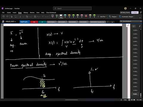
Lecture 28: Intro to noise; Input referred noise voltage and current
View
Lecture 27(2): Common-mode to differential-mode conversion in diff amp & offset due to mismatch
View
Lecture 27(1): Mismatch in current mirror
View
Lecture 26(2): Random mismatch & process variations; Relative mismatch; Pelgrom's model
View
Lecture 26(1): Fully differential two stage feedforward compensated OTA with current reuse
View
Lecture 25: Common-mode rejection by CMFB & output impedance due to CMFB
View
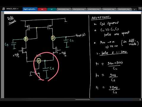
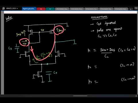
Lecture 24(2): Fully differential two-stage Miller compensated OTA with CMFB design considerations
View
Lecture 24(1): CMFB variants (contd.)
View
Lecture 23: Common-mode feedback variants
View
Lecture 22(2): Need for common-mode feedback in fully differential opamps
View
Lecture 22(1): Power supply rejection ratio of 5-transistor OTA; Need for differential signaling
View
Lecture 21(2): Nested Miller & Feedforward compensation
View
Lecture 21(1): So far in this course... A 26 minute recap
View
Lecture 20(2): Feedforward compensation; comparison with Miller compensation
View
Lecture 20(1): Ahuja compensation (contd.): Circuit implementation
View
Lecture 19(2): Ahuja compensation: Pole locations; Intuition for complex poles in Ahuja compensation
View
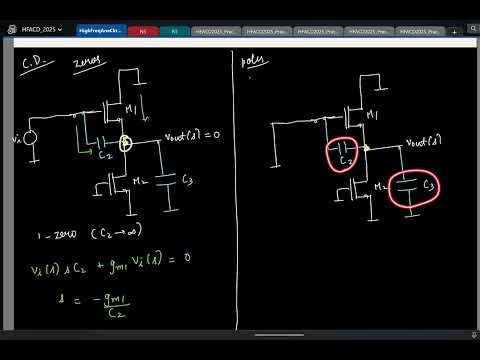
Lecture 19(1): Miller compensation: Adding a series resistor to eliminate RHP zero
View
Lecture 18: Miller OTA: Circuit implementation; Need for DC negative feedback; Systematic offset
View
Lecture 17(2): Rough design example of the two-stage Miller compensated OTA
View
Lecture 17(1): Introducing the two-stage Miller compensated OTA
View
Lecture 16(3): Understanding Miller & feed-forward compensation from root-locus
View
Lecture 16(2): Time-domain perspective on why LHP zeros are good & RHP zeros are bad for stability
View
Lecture 16(1): Time-domain understanding on why more poles makes the closed-loop system unstable?
View
Lecture 15: Deriving phase margin from root locus; Loop gain more than one & 180deg phase: stable?
View
Lecture 14(3): Need for multi-stage OTAs; 1st order systems in negative feedback
View
Lecture 14(2): Poles & zeros in telescopic cascode
View
Lecture 14(1): Detecting uncoupled poles; Summary on when to write pole as conductance by cap.
View
Lecture 13(4): Poles and zeros in cascode
View
Lecture 13(3): 5-transistor OTA: Summary of poles & zeros in differential mode
View
Lecture 13(2): Zeros in differential mode in the five-transistor OTA (pole-zero cancellation)
View
Lecture 13(1): Pole locations in the five-transistor OTA
View
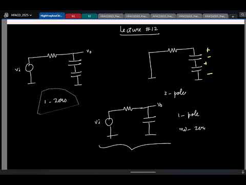
Lecture 12(5): Intuition for high-freq. pole. Why can't Miller effect be used for high-freq. pole?
View
Lecture 12(4): Miller effect: Intuition behind low-frequency pole location in common-source config.
View
Lecture 12(3): Poles & zeros in common-source configuration
View
Lecture 12(2): Poles & zeros by inspection in common-drain configuration
View
Lecture 12(1): Poles & zeros (recap); example of an uncontrollable and unobservable state
View
Lecture 11(2): Test to find presence of zeros; Origin of zeros; Calculating zero location
View
Lecture 11(1): Pole location; When can poles be approx as ratio of conductance & cap.?
View
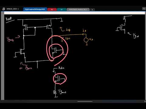
Lecture 10(2): Gain-boosted cascode; Gm boosting
View
Lecture 10(1): Slew rate of a folded cascode OTA
View
Lecture 9(1): Motivation for folded cascode opamp; Telescopic cascode opamp in unity feedback
View
Lecture 9(2): Merits of folded-cascode: Input common-mode range, output range, unity feedback swings
View
Lecture 8: Telescopic cascode: DC op. point, dc gain, input common-mode range & output swing limits
View
Lecture 7: Systematic design of analog circuits using look-up tables (gm/Id based) & design example
View
Lecture 6(3): Common mode & differential mode response of the 5-transistor OTA
View
Lecture 6(2): Impedances at each node in the 5-transistor OTA
View
Lecture 6(1): Example problems; Defining the impedance looking up and down into a node
View
Lecture 5(2): Slew rate of the five-transistor OTA
View
Lecture 5(1): Step response of a VCCS vs. VCVS in negative feedback with a capacitive load
View
Lecture 4(3): Input common-mode range and output range calculations in the five-transistor OTA
View
Lecture 4(2): Why input common-mode & output range are relevant in opamps?
View
Lecture 4(1): Summary of differential amplifier; OTA vs opamp
View
Lecture 3(3): The 5-transistor amplifier: Short-circuit transconductance & output resistance
View
Lecture 3(2): The five-transistor amplifier: DC operating point
View
Lecture 3(1): Differential amplifier: Differential mode & common-mode half circuits
View
Lecture 2: Recap of Common source, drain & gate configurations; Re-intro to differential amplifier
View
Lecture 1: MOSFET recap: Strong inversion vs. weak inversion vs. linear region; Universality of VCCS
View