AnalogLore
Playlists
Search
Vault
Playlists
Search
Vault
arrow_back
All playlists
SSCD IIT Kanpur
·
Basic Analog Building Blocks
·
45 videos
EE370: Digital Electronics (2025)
Original playlist on YouTube
arrow_outward
Videos in this playlist
EE370 Lec1: Overview of digital design implementation (Introductory lecture)
View
EE370 lec2: Verilog (I)
View
EE370 lec3: Verilog - (II)
View
EE370 lec4: Verilog - (III)
View
EE370 lec5: Verilog (IV)
View
EE370 lec6: Mealy vs Moore state machines
View
EE370 lec7: State minimization in FSM, FSMD
View
EE370 lec 8 (1) : Introduction to FSM and datapath
View
EE370 lec 8 (2): FSMD for greatest common divisor computation
View
EE370 lec11(1) : Design of controller for a faster algorithm for GCD computation
View
EE370 lec11(2) : Verilog implementation of GCD algorithm
View
EE370 lec12: Timing analysis in a digital design
View
EE370 lec13: Static timing analysis (II)
View
EE370 lec14 (1): Review of an FSMD for modulo operation
View
EE370 lec14( 2): STA with contamination and propagation delays
View
EE370 lec15: ROM, PAL, PLA
View
EE370 lec16( 1): Tutorial problem of setup, hold and clk-to-q delays of a D-flipflop
View
EE370 lec16( 2): Wired OR in ROM (one implementation), SPLD, CPLD, FPGA
View
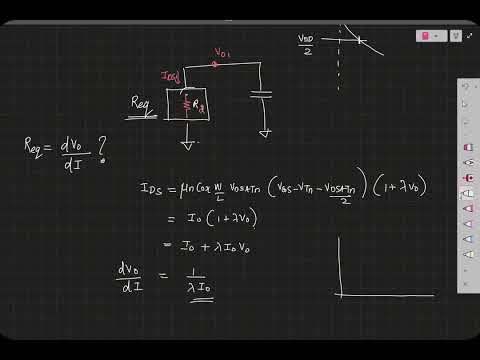
EE370 lec17: Transistor as a switch
View
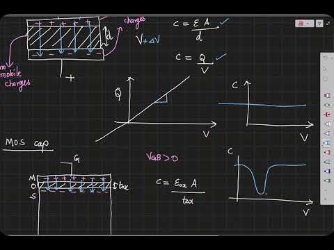
EE370 lec19: Capacitance in a MOSFET
View
EE370 lec21: Voltage Transfer Characteristics of a CMOS inverter
View
EE370 lec22: Mid-point voltage in a CMOS inverter
View
EE370 lec23: Mid-point voltage (II), Noise margin from VTC
View
EE370 lec24: Delays in a CMOS inverter (I)
View
EE370 lec25: Delays in a CMOS inverter (II)
View
EE370 lec26(1): Delays in a CMOS inverter (III)
View
EE370 lec26(2): Elmore Delay
View
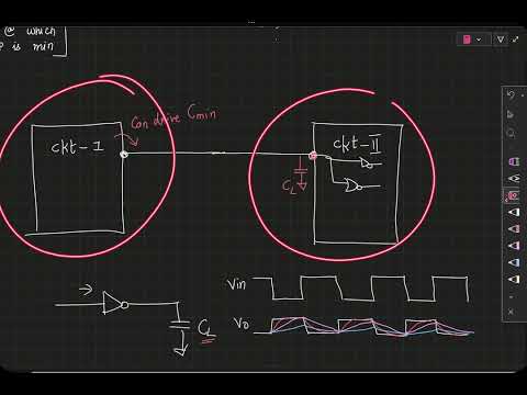
EE370 lec27: Power consumption in CMOS inverters
View
EE370 lec28: Trade-offs in optimizing power consumption in a CMOS inverter
View
EE370 lec29: Sizing an inverter chain for optimal delay
View
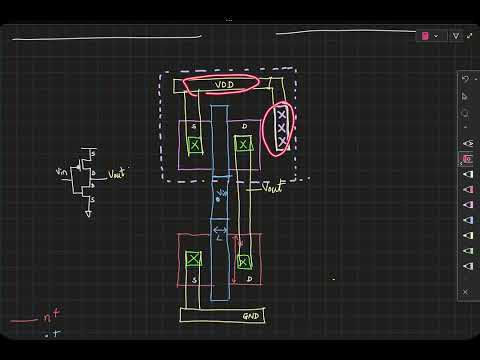
EE370 lec30: Overview of CMOS inverter layout, combinational logic
View
EE370 lec31: Sizing transistors in combinational circuits
View
EE370 lec32: Propagation and contamination delays in a combinational circuit
View
EE370 lec33(1): Fall propagation delay in N-input NAND gate
View
EE370 lec33(2): Deriving PUN from PDN using graphs
View
EE370 lec33(3): Pass transistor logic
View
EE370 lec34(1): Pass transistor logic-II
View
EE370 lec34(2): Latches and flip-flops
View
EE370 lec35: Latch implementation using transmission gates; Bistable element
View
EE370 lec36(1): Timing parameters of a flipflop built using TGs and bistable elements
View
EE370 lec36(2): Introduction to adder circuits
View
EE370 lec37: Ripple carry adder
View
EE370 lec38: Carry bypass adder
View
EE370 lec39(1): Carry select adder
View
EE370 lec39(2): EE370 done! What next?
View